Study helps understand why a material’s behavior changes as it gets smaller
Mar 09, 2015 — Atlanta, GA

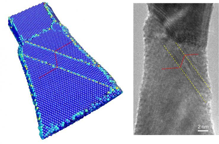
The computer model (left) and experimental image reveal atomic-level deformation twinning in a tungsten nanowire under axial compression. The lattice of the deformation-induced twin band (between yellow lines) is a mirror image of that of the parent crystal. (Courtesy Ting Zhu)
To fully understand how nanomaterials behave, one must also understand the atomic-scale deformation mechanisms that determine their structure and, therefore, their strength and function.
Researchers at the University of Pittsburgh, Drexel University and the Georgia Institute of Technology have engineered a new way to observe and study these mechanisms and, in doing so, have revealed an interesting phenomenon in a well-known material, tungsten. The group is the first to observe atomic-level deformation twinning in body-centered cubic (BCC) tungsten nanocrystals.
The team used high-resolution transmission electron microscope (TEM) and sophisticated computer modeling to make the observation. This work, published March 9 in the journal Nature Materials, represents a milestone in the in-situ study of mechanical behaviors of nanomaterials.
Deformation twinning is a type of deformation that, in conjunction with dislocation slip, allows materials to permanently deform without breaking. In the process of twinning, the crystal reorients, which creates a region in the crystal that is a mirror image of the original crystal. Twinning has been observed in large-scale BCC metals and alloys during deformation. However, whether twinning occurs in BCC nanomaterials or not remained unknown.
“To gain a deep understanding of deformation in BCC nanomaterials, we combined atomic-scale imaging and simulations to show that twinning activities dominated for most loading conditions, due to the lack of other shear deformation mechanisms in nanoscale BCC lattices.” said Scott Mao, a professor in the Swanson School of Engineering at the University of Pittsburgh.
The team chose tungsten as a typical BCC crystal. The most familiar application of tungsten is their use as filaments for light bulbs.
The observation of atomic-scale twinning was made inside a TEM. This kind of study has not been possible in the past, due to difficulties of making BCC samples less than 100 nanometers in size, as required by TEM imaging. Jiangwei Wang, a graduate student at University of Pittsburgh, and Mao, the lead author of the paper, developed a clever way of making the BCC tungsten nanowires. Under a TEM, Wang welded together two small pieces of individual nanoscale tungsten crystals to create a wire about 20 nanometers in diameter. This wire was durable enough to stretch and compress while Wang observed the twinning phenomenon in real time using a high-resolution TEM.
To better understand the phenomenon observed by Mao and Wang’s team at the University of Pittsburgh, Christopher Weinberger, an assistant professor in Drexel’s College of Engineering, developed computer models that show the mechanical behavior of the tungsten nanostructure – at the atomic level. His modeling allowed the team to see the physical factors at play during twinning. This information will help researchers theorize why it occurs in nanoscale tungsten and plot a course for examining this behavior in other BCC materials.
“We’re trying to see if our atomistic-based model behaves in the same way as the tungsten sample used in the experiments, which can then help to explain the mechanisms that allow it to behave that way,” Weinberger said. “Specifically, we’d like to explain why it exhibits this twinning ability as a nanostructure, but not as a bulk metal.”
In concert with Weinberger’s modeling, Ting Zhu, an associate professor in the Woodruff School of Mechanical Engineering at Georgia Tech, worked with a graduate student, Zhi Zeng, to conduct advanced computer simulations, using molecular dynamics to study deformation processes in 3-D.
Zhu’s simulation revealed that tungsten’s “smaller is stronger” behavior is not without drawbacks when it comes to application.
“If you reduce the size to the nanometer scale, you can increase strength by several orders or magnitude,” Zhu said. “But the price you pay is a dramatic decrease in the ductility.
We want to increase the strength without compromising the ductility in developing these nanostructured metals and alloys. To reach this objective, we need to understand the controlling deformation mechanisms.”
The twinning mechanism, Mao added, contrasts with the conventional wisdom of dislocation nucleation-controlled plasticity in nanomaterials. The results should motivate further experimental and modeling investigation of deformation mechanisms in nanoscale metals and alloys, ultimately enabling the design of nanostructured materials to fully realize their latent mechanical strength.
"Our discovery of the twinning dominated deformation also opens up possibilities of enhancing ductility by engineering twin structures in nanoscale BCC crystals" Zhu said.
Research News
Georgia Institute of Technology
177 North Avenue
Atlanta, Georgia 30332-0181
Media Relations Contacts: Georgia Tech – John Toon (404-894-6986) (jtoon@gatech.edu) or the University of Pittsburgh – Joe Miksch (412-624-4356) (jmiksch@pitt.edu).
Writer: Joe Miksch, University of Pittsburgh

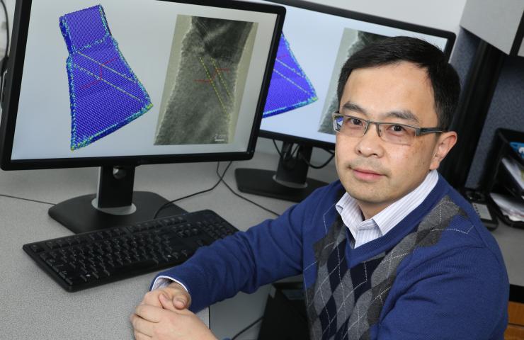
Ting Zhu, an associate professor in Georgia Tech’s Woodruff School of Mechanical Engineering, worked with colleagues at the University of Pittsburgh and Drexel University to develop a better understanding of a key deformation mechanism in nanoscale tungsten. (Credit: Candler Hobbs)


