Researchers Lead Microelectronics Advances from Lab-to-fab, Bolstered by Synergy with GTRI
Dec 16, 2021 — Atlanta, GA
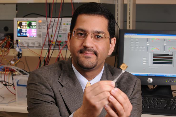
Muhannad Bakir, a professor in the School of Electrical and Computer Engineering, holding a monolithic microelectronics chip. He brings a breadth of knowledge to the shift from monolithic microelectronics to heterogeneous integration. (Photo credit: Robert Felt, Georgia Tech)
A hotbed for semiconductor innovation, the Georgia Institute of Technology offers deep domain expertise in device and integration technologies, as well as high-assurance tools for chip security. The Institute, along with Georgia Tech Research Institute (GTRI), leads in areas such as emerging materials/devices, innovative circuit/architectures, and advanced integration and packaging.
“One thing I love about Georgia Tech is that you have expertise in every single aspect of electronics,” said Muhannad Bakir, Dan Fielder electrical engineering professor in the School of Electrical and Computer Engineering. “If I have questions on materials, devices, architectures, circuits, or even software compilers, I don’t have to look far. I turn a corner and there is that expert for you.”
Monolithic to Heterogeneous Electronics Integration
Bakir credited this breadth of knowledge at Georgia Tech with helping the Institute be a leader in shifting from monolithic microelectronics to “heterogeneous” integration. In this type of integration, separately manufactured components become part of a higher-level assembly that, in total, provides enhanced functionality and improved operating characteristics for applications.
“We have to look at a whole host of issues in order to continue to drive cost, performance and energy benefits going forward,” explained Bakir as to the reasons behind this development.
His team is identifying and optimizing the processes and materials of different microelectronic components to get the most out of each one. They then are integrating the different pieces into a single, high-performing system. Specifically, Bakir is developing new ways to glue or wire these interconnect technologies together in a way that maximizes their performance.
“With most high-power applications, heat is a huge problem. As you build your stack by mounting multiple chips on top of each other within a single semiconductor package, you really need to think about innovative cooling strategies,” said Bakir. “What you see today is a lot of mixing and matching of different technologies, each optimized for the function they’re performing”
To address this challenge, the Integrated 3D systems (i3DS) Lab, which Bakir directs, is working on novel chip-level microfluidic cooling techniques to enhance heat removal, an area in which Georgia Tech has unique expertise and capabilities. Georgia Tech engineering faculty have won multiple large-scale funded research grants in embedded microfluidic cooling for electronic applications, including 3D chip stacking. The teams demonstrated Georgia Tech's ability to drive advanced cooling technology solutions from fundamental design to manufacturing and integration on leading-edge electronic silicon-testbeds using in-house Georgia Tech facilities.
Bakir’s lab is also working on novel “stitch-chips” that provide a high-speed connection between neighboring chips in a package by avoiding the traditional slow interconnection through a package with high electrical losses.
Bakir considers GTRI “an incredible asset to what we do.” “They have some unique design and fabrication capabilities. Equally important is the fact that GTRI is well known internationally for being able to deliver technologies that are truly differentiated and based on unique designs and processes that we develop inhouse,” Bakir said.
High-Assurance Tools to Assess Chip Vulnerabilities
One of those partners includes Lee Lerner, chief scientist of GTRI’s Cybersecurity, Information Protection and Hardware Evaluation Research (CIPHER) Laboratory. Lerner’s Lab develops third-party tools to conduct high-assurance microelectronics inspections for global customers like Intel and Defense Advanced Research Projects Agency (DARPA) on the defense side. His team focuses on high-assurance inspection through testing technologies that provide “assurance of trust,” or peace of mind that these systems perform as expected.
“We can tell you that the tools and devices are actually doing what they're supposed to do and nothing more,” Lerner said.
An additional challenge in this space is that the current chip shortage creates more demand on older chip technologies, which have less security features or more known vulnerabilities than modern devices.
GTRI develops some of the most advanced IP and electronic security protections and features in existence. Because of this work, researchers understand which security features work and which are insufficient given the growing complexity and types of attacks at the hardware level.
According to Lerner, GTRI is making big investments over the next 10 years in building security and trust for microelectronics. In fact, the Institute’s strategic roadmap includes trusted microelectronics as a key pillar.
Increased Cybersecurity Focus
Georgia Tech is also making big investments, such as establishing the new School of Cybersecurity and Privacy, and hiring expert faculty such as Daniel Genkin, associate professor, who officially reported on Meltdown and Spectre, two of the most widely publicized vulnerabilities in the last decade involving chips in popular devices. In addition to Lerner and Genkin, Alenka Zajić, Ken Byers Professor in Electrical and Computer Engineering, has pioneered novel inspection techniques of microelectronics.
“Having a good understanding of the true state of the art of security and trust features, as well as bleeding-edge vulnerabilities, help inform future generations of security protections that need to be incorporated into more devices generally, including approaches to design, so that we don't encounter those types of vulnerabilities,” he said.
Lee says more customers are paying attention to the importance of security flaws in designs and potential vulnerabilities. “They're increasingly investing more, but there still are competing factors of designing for security versus designing for performance,” he added.
He emphasized that microelectronics is fundamentally hardware, which is very expensive to change once it’s fabricated and manufactured. “If big flaws or security exploits are discovered, it's not easy to go back and distribute patches to those systems. Those flaws live on in the microelectronics… sometimes for decades in even critical systems,” Lee noted. That’s where Georgia Tech and GTRI can be a valuable partner, by contributing security and design for trust “very early on in either materials or architectures that improve trust and reliability of devices.”
On the chip innovation side, Georgia Tech faculty are leveraging the institute’s multidisciplinary strengths and semiconductor facilities to solve semiconductor development bottlenecks and improve the performance of chip technologies.
Driving In-Memory Computing
One such innovator is Shimeng Yu, associate professor in Electrical and Computer Engineering, whose work on “in-memory compute” could solve the hardware bottleneck in today’s data-intensive applications that increasingly rely on machine learning and artificial intelligence.
“Data storage is becoming more important these days. There’s so much data and information from sensors and cameras, we want to do the computation locally using the data within the memory to save on data transfer energy and bandwidth,” Yu explained.
“The memory market today focuses exclusively on data storage, and memory is expensive, accounting for nearly a third of the cost of a chip,” said Yu. His pioneering work merging the compute function with data storage is 10 times more energy-efficient than conventional approaches where data is fetched from a centralized data processor.
To realize this new computing paradigm, Yu and his team are working with the Packaging Research Center (PRC) to package their solution into a prototype and ultimately, a complete system. Their work depends on the ability to innovate at the material/device level and translate those innovations into circuits for prototype demonstrations.
“The capability to facilitate this kind of lab-to-fab tech transfer is critical,” said Yu.
While his team can explore new materials and standalone device structures in the Georgia Tech cleanroom, “we need a prototyping facility to enable large-scale, array-level demonstration for new memory technologies,” he said. “The PRC is going to help us get there, packaging our prototype into a complete system.”
“The PRC enables the heterogeneous integration of our new device technologies with commercial off-the-shelf silicon chips from commercial foundries,” he added.
Yu said his in-memory compute breakthrough is creating excitement among both traditional chip makers and non-traditional companies looking to build their own silicon chips such as Google, Facebook, Microsoft, Amazon, and Tesla.
***
The Georgia Institute of Technology, or Georgia Tech, is a top 10 public research university developing leaders who advance technology and improve the human condition. The Institute offers business, computing, design, engineering, liberal arts, and sciences degrees. Its nearly 44,000 students representing 50 states and 149 countries, study at the main campus in Atlanta, at campuses in France and China, and through distance and online learning. As a leading technological university, Georgia Tech is an engine of economic development for Georgia, the Southeast, and the nation, conducting more than $1 billion in research annually for government, industry, and society.
Writer: Anne Wainscott-Sargent

(L to R): Bill Hunter, Mike Ruiz, Chris Clark, Jay Danner, Will Stuckey and Lee W. Lerner -- the leadership team of a division of faculty at GTRI, which advances applied research in hardware security and trust. (Photo credit: Christopher Moore, Georgia Tech)

Georgia Tech Associate Professor Shimeng Yu’s lab members (the two on right) perform semiconductor device testing on probe stations. Yu is helping solve the memory processing bottleneck issue. Merging the compute function with data storage in devices leads will improve energy and bandwith effiiencies by a factor of 10. (Photo credit: Shimeng Yu, Georgia Tech)

A 300mm silicon wafer with advanced memory technologies from Georgia Tech’s industry partner for device characterization to be performed at Georgia Tech’s facilities. (Photo credit: Shimeng Yu, Georgia Tech)
Anne Wainscott-Sargent


