Researchers Create Faster and Cheaper Way to Print Tiny Metal Structures With Light
Jan 18, 2024 —
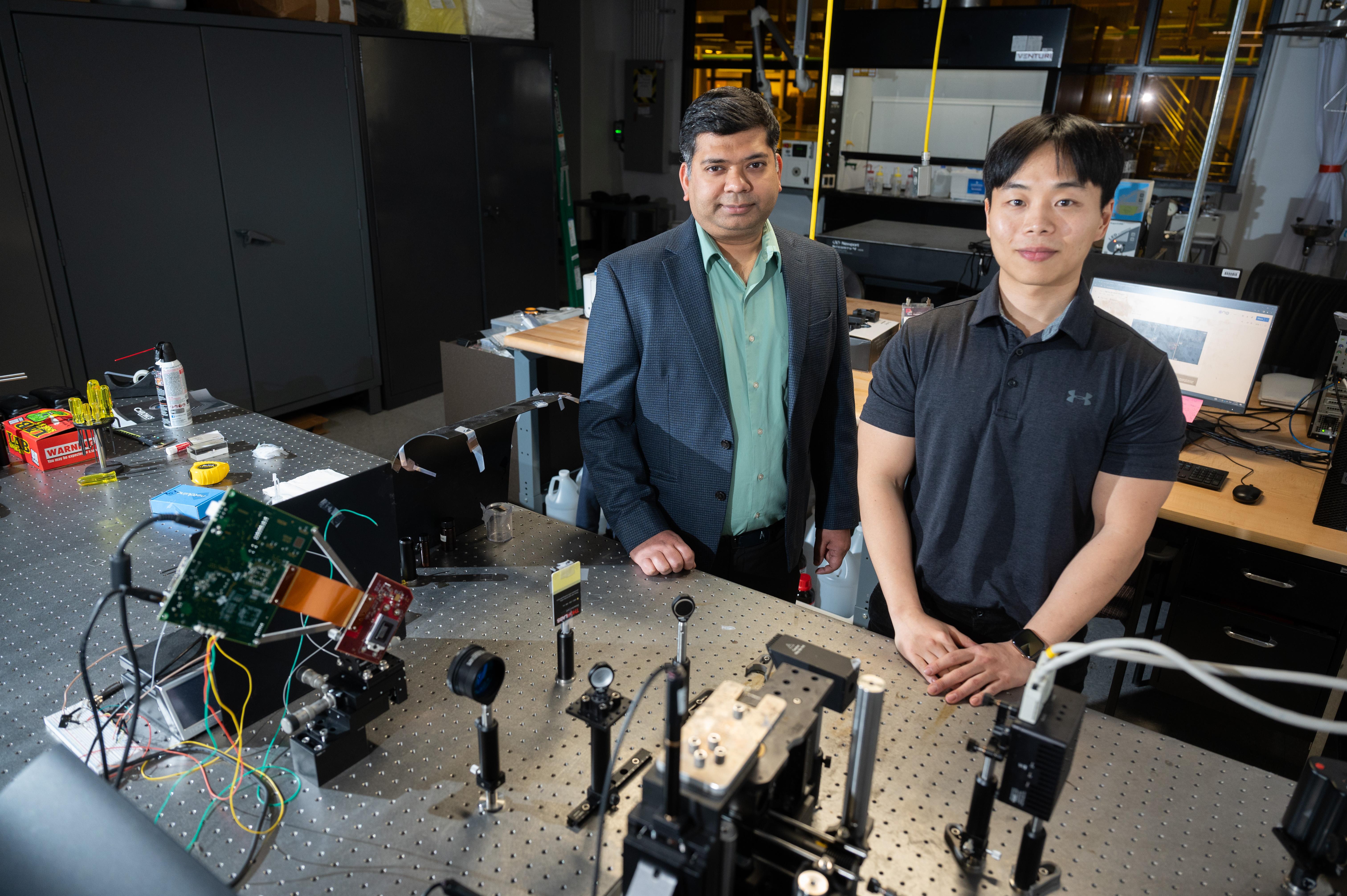
Assistant professor Sourabh Saha and Jungho Choi (Ph.D. student) in front of their superluminescent light projection system at Georgia Tech. Credit: Allison Carter
Researchers at the Georgia Institute of Technology have developed a light-based means of printing nano-sized metal structures that is significantly faster and cheaper than any technology currently available. It is a scalable solution that could transform a scientific field long reliant on technologies that are prohibitively expensive and slow. The breakthrough has the potential to bring new technologies out of labs and into the world.
Technological advances in many fields rely on the ability to print metallic structures that are nano-sized — a scale hundreds of times smaller than the width of a human hair. Sourabh Saha, assistant professor in the George W. Woodruff School of Mechanical Engineering, and Jungho Choi, a Ph.D. student in Saha’s lab, developed a technique for printing metal nanostructures that is 480 times faster and 35 times cheaper than the current conventional method.
Their research was published in the journal Advanced Materials.
Printing metal on the nanoscale — a technique known as nanopatterning — allows for the creation of unique structures with interesting functions. It is crucial for the development of many technologies, including electronic devices, solar energy conversion, sensors, and other systems.
It is generally believed that high-intensity light sources are required for nanoscale printing. But this type of tool, known as a femtosecond laser, can cost up to half a million dollars and is too expensive for most research labs and small businesses.
“As a scientific community, we don’t have the ability to make enough of these nanomaterials quickly and affordably, and that is why promising technologies often stay limited to the lab and don’t get translated into real-world applications,” Saha said.
“The question we wanted to answer is, ‘Do we really need a high-intensity femtosecond laser to print on the nanoscale?’ Our hypothesis was that we don’t need that light source to get the type of printing we want.”
They searched for a low-cost, low-intensity light that could be focused in a way similar to femtosecond lasers, and chose superluminescent light emitting diodes (SLEDs) for their commercial availability. SLEDs emit light that is a billion times less intense than that of femtosecond lasers.
Saha and Choi set out to create an original projection-style printing technology, designing a system that converts digital images into optical images and displays them on a glass surface. The system operates like digital projectors but produces images that are more sharply focused. They leveraged the unique properties of the superluminescent light to generate sharply focused images with minimal defects.
They then developed a clear ink solution made up of metal salt and added other chemicals to make sure the liquid could absorb light. When light from their projection system hit the solution, it caused a chemical reaction that converted the salt solution into metal. The metal nanoparticles stuck to the surface of the glass, and the agglomeration of the metal particles creates the nanostructures. Because it is a projection type of printing, it can print an entire structure in one go, rather than point by point — making it much faster.
After testing the technique, they found that projection-style nanoscale printing is possible even with low-intensity light, but only if the images are sharply focused. Saha and Choi believe that researchers can readily replicate their work using commercially available hardware. Unlike a pricey femtosecond laser, the type of SLED that Saha and Choi used in their printer costs about $3,000.
“At present, only top universities have access to these expensive technologies, and even then, they are located in shared facilities and are not always available,” Choi said. “We want to democratize the capability of nanoscale 3D printing, and we hope our research opens the door for greater access to this type of process at a low cost.”
The researchers say their technique will be particularly useful for people working in the fields of electronics, optics, and plasmonics, which all require a variety of complex metallic nanostructures.
“I think the metrics of cost and speed have been greatly undervalued in the scientific community that works on fabrication and manufacturing of tiny structures,” Saha said.
“In the real world, these metrics are important when it comes to translating discoveries from the lab to industry. Only when we have manufacturing techniques that take these metrics into account will we be able to fully leverage nanotechnology for societal benefit.”
Citation: J. Choi, S. K. Saha, Scalable Printing of Metal Nanostructures through Superluminescent Light Projection. Adv. Mater. 2024, 36, 2308112.
DOI: https://doi.org/10.1002/adma.202308112
Funding: Funding includes grants from the G.W.W. School of Mechanical Engineering and the EVPR’s office at the Georgia Institute of Technology. Imaging was performed at the Georgia Tech Institute for Electronics and Nanotechnology, a member of the National Nanotechnology Coordinated Infrastructure (NNCI), which is supported by the National Science Foundation (ECCS-2025462).
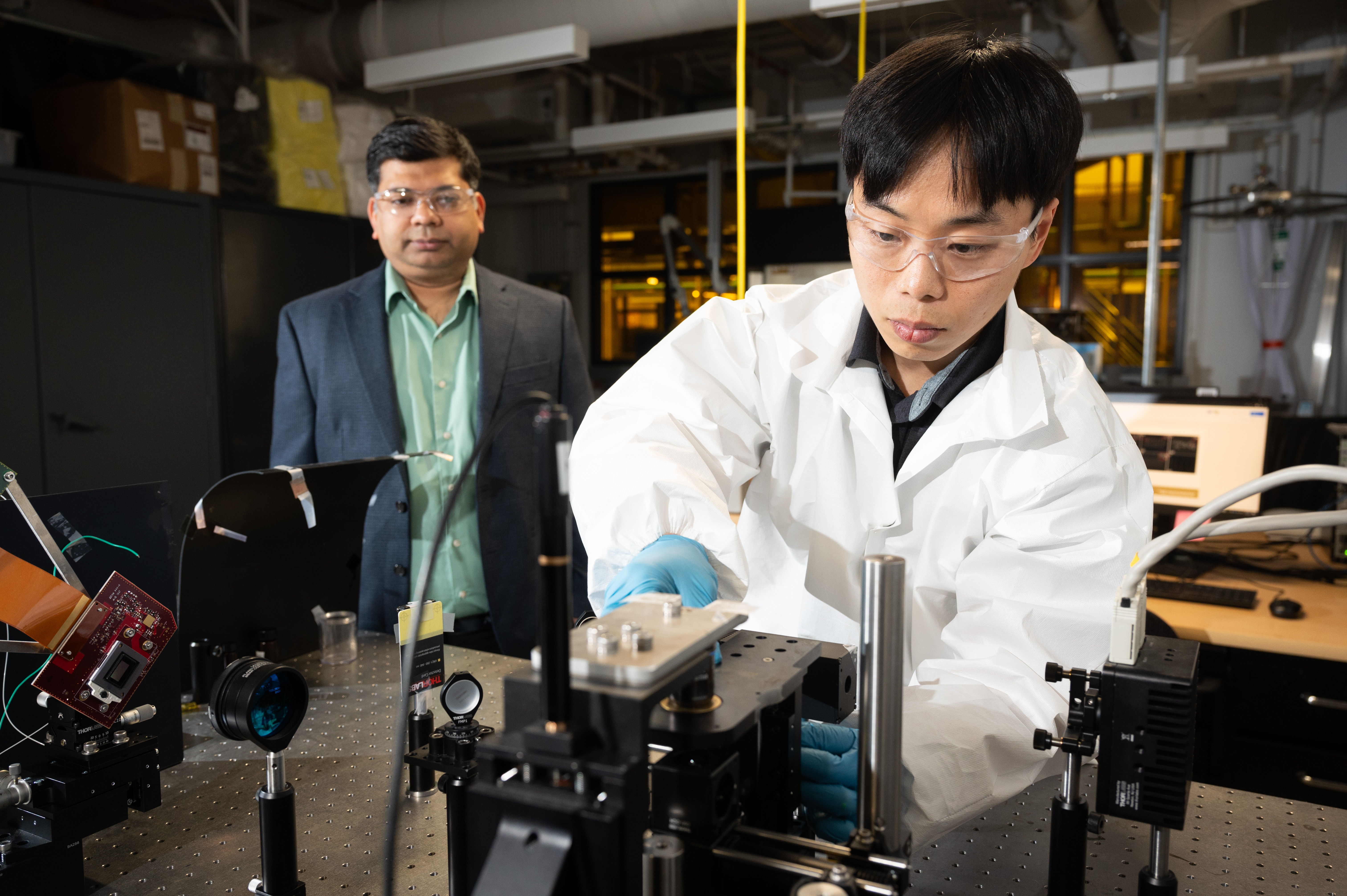
Ph.D. student Jungho Choi controlling LED brightness levels on the SLP system. Credit: Allison Carter
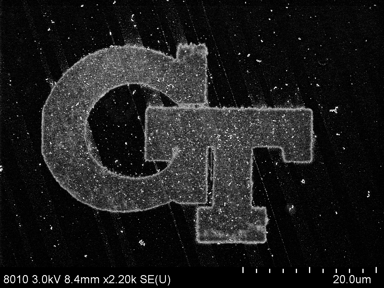
Scanning electron microscope image of a printed silver Georgia Tech logo made with the researchers' SLP technique. Credit: Jungho Choi
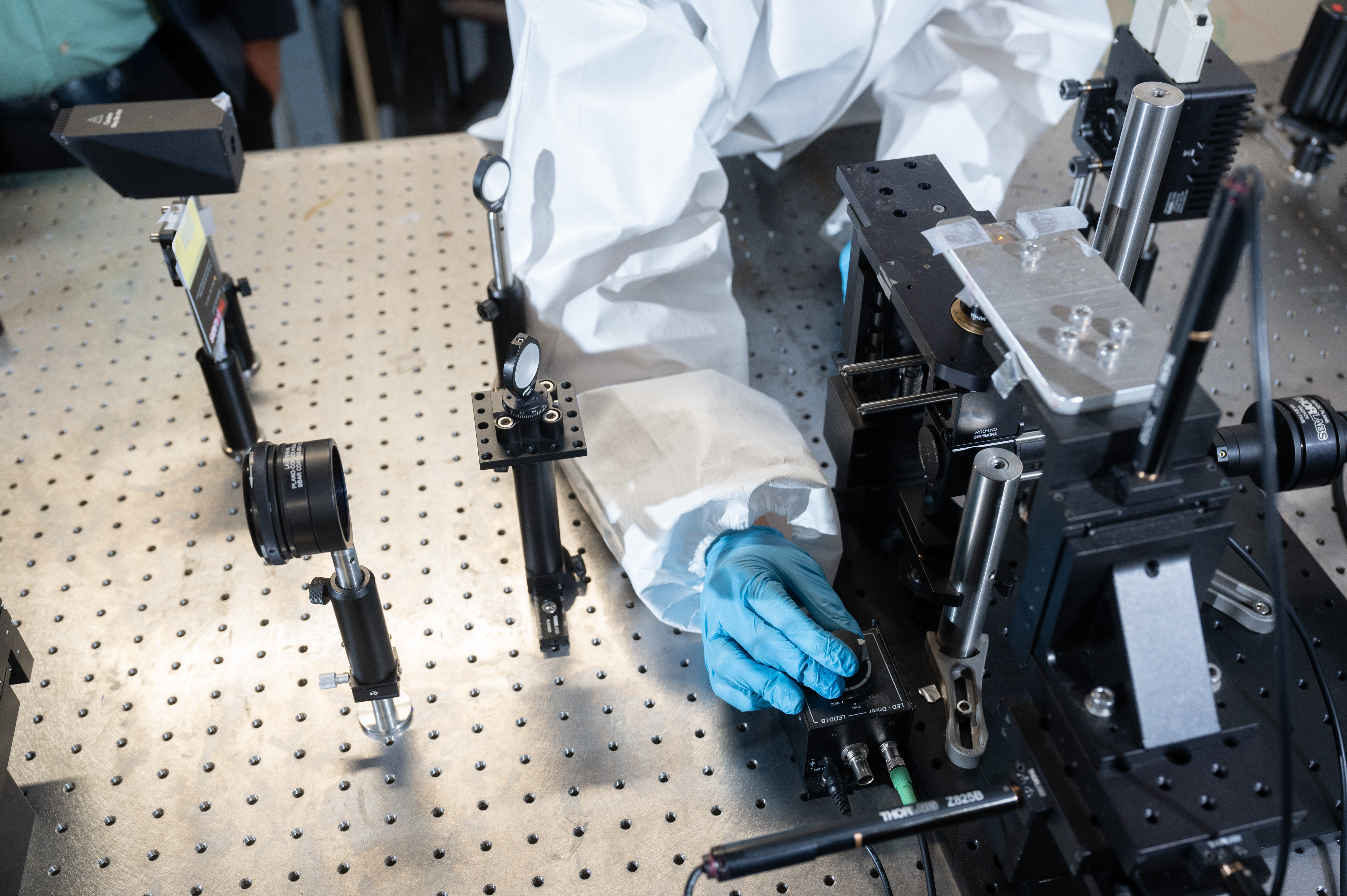
Choi (right) carries out optical adjustment for the correct focal plane of the SLP system. Credit: Allison Carter
Catherine Barzler, Senior Research Writer/Editor


