Georgia Tech’s New Aluminum Nitride-based Semiconductor is Poised to Transform the Industry
Aug 04, 2022 — Atlanta, GA

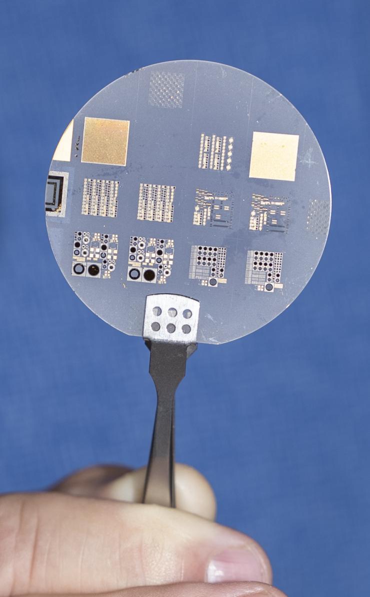
ECE professor Alan Doolittle’s AlN-based semiconductor findings represent an emerging new area of interdisciplinary research covering materials, physics, and devices.
Alan Doolittle is doing what was once thought impossible: turning an electrical insulator into an ultra-wide bandgap semiconductor. The results have groundbreaking potential for high-power electronics, optoelectronics, and more.
For the past 80 or so years, aluminum nitride (AlN) has been thought of as nothing but an electrical insulator. Because of its high electrical insulating and thermal conductivity properties, it is used frequently in electronic applications to dissipate heat quickly and maintain efficiency.
Researchers at the Georgia Institute of Technology, led by professor Alan Doolittle, are discovering that there is a lot more to AlN than meets the eye, and their promising research shows the material has the potential to transform the semiconductor industry. By leveraging the advantages of AlN, ultra-wide bandgap (UWBG) semiconductors can be used at high-power and high-temperature levels never seen before.
“It’s rare to see such encouraging early results,” said Doolittle, the Joseph M. Pettit Professor in the School for Electrical and Computer Engineering (ECE). “To put things into perspective, AlN has the ability to handle over five times the voltage of other existing wide bandgap semiconductors. It really is the birth of a new semiconductor field.”
For electrical devices, there are two types of semiconducting materials needed: one that carries positive charges (p-type) and one that carries negative charges (n-type). The Doolittle group was able to improve current conduction in p-type AlN by 30,000,000 times and n-type AlN by 6,000 times than prior best results.
The findings, recently published in Advanced Materials and the Journal of Applied Physics, received the Most Valuable Contribution Award at the 2022 Workshop on Compound Semiconductor Materials & Devices, a premier workshop in the U.S. on high performance electronic materials.
Ultra-wide Bandgaps Equal Ultra-wide Applications
Georgia Tech’s AlN-based semiconductor findings represent an emerging new area of interdisciplinary research covering materials, physics, and devices with promising applications for future generations of high-power electronics and optoelectronics, as well as quantum electronics and harsh-environment applications.
Semiconductors can both conduct and insulate electricity, meaning they are necessary for all electronic appliances to operate. Scientists make semiconductor materials by using pure elements (most frequently silicon) and adding intentional impurities to make crystals with the desired electrical, thermal, and optical prosperities.
The bandgap is one of the most important properties of a semiconductor, as it represents the minimum energy required for electrical conduction. It is also the largest factor in determining the voltage at which a device fails (called breakdown), as well as represents the energy/wavelength of light emanating from the semiconductor. UWBG semiconductors can operate at high temperatures, frequencies, and voltages, meaning less semiconductor devices are needed in high voltage circuits which increases performance and efficiency, while reducing costs. Doolittle’s AlN-based semiconductor has the highest bandgap ever demonstrated to have both p and n-type conduction needed for electronics.
“The new AlN-based semiconductor appears to have the ability to withstand voltages at incredibly high levels,” said Doolittle. “Levels that can even withstand some sections of the national utility grid, something no other semiconductor can do.”
With the ability to withstand high voltage and high frequency, AlN-based semiconductors can be utilized in power electronic devices found in automotive, industrial, and consumer applications. The technology could also allow utility grids to more effectively control how much power to transmit and where, a growing demand as old systems integrate with other smart grid innovations and renewable energy sources.
The team used a much lower temperature to grow the AlN crystals than what is normally utilized to create semiconductor materials. The low heat process allows for more precise control of the material’s surface chemistry during creation and is potentially a groundbreaking innovation in its own right.
“That kind of out of the box solution caught a lot of people off guard,” said Doolittle. “It was thought that you couldn’t grow good quality material at this low of temperature, but we’ve shown that it’s possible and has broad applicability.”
AlN’s Impressive Optical Properties
Unlike an incandescent light bulb where a filament is heated to glow and produce light, light-emitting diodes (LEDs) emit light when an electric current flows through a layered semiconductor device. The wide bandgap semiconductor material gallium nitride (GaN) was used to create the first LED blue light in the early 1990s by Isamu Akasaki, Hiroshi Amano, and Shuji Nakamura (for which they won the 2014 Nobel Prize in Physics). Creating the high energy blue LED challenged scientist for decades, as it was the final piece needed to create white light and full-color LED displays that have now revolutionized lighting technology and is predicted to save nearly 20% in energy consumption in the U.S. when fully deployed.
Like GaN, AlN’s wide bandgap means it has enormous light energy which results in the short light wavelengths needed to produce high energy deep ultra-violet (DUV) light beyond the ability of the eye to see. Because AlN has an even larger bandgap than GaN, it produces a DUV light with a wavelength of only 203 nanometers (compared to GaN’s ~365 nm) – nearly twice the energy as light from GaN.
“We're really excited about the optical properties of this material,” said Doolittle. “Researchers have been attempting to get LEDs under 270 nanometer wavelengths for a while now because it opens up an enormous range of applications.”
One such potential application for AlN-based LEDs is light disinfection, a growing focus in research and industry. Unlike current ultraviolet (UV) lights — a light disinfectant plagued by power/efficiency limitations — DUV LEDs use higher energy electromagnetic radiation that is absorbed in the dead layers of human skin instead of being absorbed in live tissue.
“This light gives us a pathway to make light emitters that can kill viruses and bacteria with significantly less — if any — damage to human skin and eyes.” said Doolittle.
Time to Engineer
With the team’s encouraging early studies showing AlN having the potential to be a revolutionary semiconductor material, they now turn to prototyping and optimization. While the new technology is a leap forward and largely solves the most difficult science problems that have roadblocked using AlN as a semiconductor, engineering challenges remain.
Since such a wide bandgap semiconductor has never been created, a solution to make good electrical contact to the material (for electrical current to be transported to devices) is essential. All known metals are poorly suited to contact AlN, so metal alloys and exotic contacts will be needed, according to Doolittle.
Early prototypes have shown some resistance to current flow that must be improved if AlN is to reach the efficiencies it potentially can achieve. Likewise, thicker devices will need to be engineered to use in the high voltages needed to impact utility grids.
“We have ideas as to how to push this forward and view most of these issues as engineering challenges requiring only time and resources, not fundamental science limitations,” said Doolittle.
***
Citation I: H. Ahmad, J. Lindemuth, Z. Engel, C. M. Matthews, K. Motoki, W. Alan Doolittle, “Substantial P-type Conductivity of AlN Achieved via Beryllium Doping,” Advanced Materials 33 (42), 2104497, September 2021.
DOI: doi.org/10.1002/adma.202104497
Citation II: H. Ahmad, Z. Engel, C. M. Matthews, S. Lee, and W. Alan Doolittle, “Realization of homojunction PN AlN diodes”, J. Appl. Phys. 131, 175701 (2022)
DOI: doi.org/10.1063/5.0086314
Funding: This work was supported by the Office of Naval Research (ONR) Multidisciplinary University Research Initiatives (MURI) Program entitled, “Leveraging a New Theoretical Paradigm to Enhance Interfacial Thermal Transport In Wide Bandgap Power Electronics” under Award No. N00014-17-S-F006 administered by Dr. Mark Spector and Lynn Petersen. This work was also in part supported by the Air Force Office of Scientific Research under Award number FA9550-21-1-0318 administered by Dr. Ali Sayir.
Writer: Dan Watson
Photography: Marion Crowder
Media Contact: Dan Watson | dwatson@ece.gatech.edu
###
The Georgia Institute of Technology, or Georgia Tech, is a top 10 public research university developing leaders who advance technology and improve the human condition. The Institute offers business, computing, design, engineering, liberal arts, and sciences degrees. Its nearly 44,000 students, representing 50 states and 149 countries, study at the main campus in Atlanta, at campuses in France and China, and through distance and online learning. As a leading technological university, Georgia Tech is an engine of economic development for Georgia, the Southeast, and the nation, conducting more than $1 billion in research annually for government, industry, and society.
Georgia Tech’s AlN-based semiconductor has the highest bandgap ever demonstrated to have both p and n-type conduction needed for electronics.
Dan Watson
dwatson@ece.gatech.edu


