William Hunt

William Hunt
bill.hunt@ece.gatech.edu
Microelectronic Acoustics Group

Hunt grew up in the literary haven of Columbus, Mississippi, the boyhood home of Tennessee Williams, and received his B.S.E.E. from the University of Alabama in 1976. He worked for Harris Corporation for two years in the areas of acousto-optics and surface acoustic wave (SAW). He then entered the Massachusetts Institute of Technology where he earned his S.M.E.E. in 1980 and conducted research in the field of auditory physiology. After four years with Bolt, Beranek and Newman, Inc. he entered the University of Illinois, Champaign-Urbana where he received his Ph.D. in electrical engineering in 1987. His research there was on acoustic charge transport (ACT) devices and the SAW properties of Gallium Arsenide.

Hunt joined the faculty of the Georgia Institute of Technology in the fall of 1987 as one of the original members of the Pettit Microsystems Research Center. There he founded the Microelectronic Acoustics Group which focuses on the development of ultrasonic devices that can be integrated with Microsystems. Among these have been, ACT devices, micromachined polyvinylidene fluoride-trifluoroethylene (PVDF)-based transducers for intravascular ultrasound, acousto-optic devices for tunable lasers as well as SAW and bulk acoustic wave (BAW) devices for wireless and chemical sensor applications.

Professor, School of Electrical and Computer Engineering
Director, Microelectronic Acoustics Group
Phone
404.894.2945
Office
MiRC 221
Additional Research

Piezoelectronic Materials; Thin Films; Acoustics and Dynamics; Bio-Devices; Fabrication

Research Focus Areas
Google Scholar
https://scholar.google.com/citations?hl=en&user=z0FMakMAAAAJ&view_op=list_works&sortby=pubdate
ECE Profile Page
William
Hunt
D.
Show Regular Profile

Phillip First

Placeholder for headshot
phillip.first@physics.gatech.edu
Surface, Interface and Nanostructure Research Group

A primary goal of Professor First's research is to develop an understanding of solid-state systems at atomic length scales. The main experimental tools in this pursuit are scanning tunneling microscopy (STM) and related techniques such as ballistic electron emission microscopy (BEEM). These methods rely on the quantum-mechanical tunnel effect to obtain atomically-resolved maps of the electronic structure of surfaces, clusters, and buried layers.

Professor, School of Physics
Director, Surface, Interface, and Nanostructure Research Group
Phone
404.894.0548
Office
Howey N018/ S03
Additional Research

Electron microscopy, surfaces and interfaces, graphene, epitaxial growth

Research Focus Areas
University, College, and School/Department
Google Scholar
https://scholar.google.com/citations?hl=en&user=_KM8x1kAAAAJ&view_op=list_works&sortby=pubdate
Physics Profile Page
Phillip
First
N.
Show Regular Profile

Manos Tentzeris

Manos  Tentzeris
etentze@ece.gatech.edu
ECE Profile Page

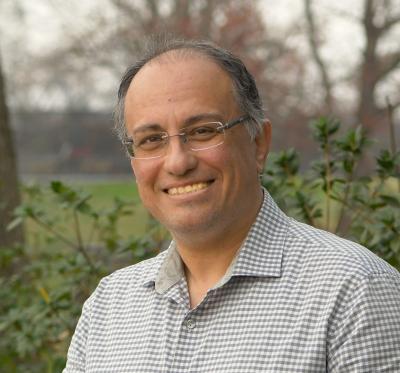
Manos Tentzeris was born and grew up in Piraeus, Greece. He graduated from Ionidios Model School of Piraeus in 1987 and he received the Diploma degree in Electrical Engineering and Computer Science (Magna Cum Laude) from the National Technical University in Athens, Greece, in 1992 and the M.S. and Ph.D. degrees in Electrical Engineering and Computer Science from the University of Michigan, Ann Arbor in 1993 and 1998. He is currently a Professor with the School of ECE, Georgia Tech and he has published more than 550 papers in refereed Journals and Conference Proceedings, 4 books and 23 book chapters, while he is in the process of writing 1 book. He has served as the Head of the Electromagnetics Technical Interest Group of the School of ECE, Georgia Tech. Also, he has served as the Georgia Electronic Design Center Associate Director for RFID/Sensors research from 2006-2010 and as the GT-Packaging Research Center (NSF-ERC) Associate Director for RF research and the leader of the RF/Wireless Packaging Alliance from 2003-2006. Also, Dr. Tentzeris is the Head of the A.T.H.E.N.A. Research Group (20 students and researchers) and has established academic programs in 3D Printed RF electronics and modules, flexible electronics, origami and morphing electromagnetics, Highly Integrated/Multilayer Packaging for RF and Wireless Applications using ceramic and organic flexible materials, paper-based RFID 's and sensors, inkjet-printed electronics, nanostructures for RF, wireless sensors, power scavenging and wireless power transfer, Microwave MEM 's, SOP-integrated (UWB, mutliband, conformal) antennas and Adaptive Numerical Electromagnetics (FDTD, MultiResolution Algorithms). He was the 1999 Technical Program Co-Chair of the 54th ARFTG Conference and he is currently a member of the technical program committees of IEEE-IMS, IEEE-AP and IEEE-ECTC Symposia. He was the TPC Chair for the IMS 2008 Conference and the Co-Chair of the ACES 2009 Symposium. He was the Chairman for the 2005 IEEE CEM-TD Workshop. He was the Chair of IEEE-CPMT TC16 (RF Subcommittee) and he was the Chair of IEEE MTT/AP Atlanta Sections for 2003. He is a Fellow of IEEE, a member of MTT-15 Committee, an Associate Member of European Microwave Association (EuMA), a Fellow of the Electromagnetics Academy, and a member of Commission D, URSI and of the the Technical Chamber of Greece. He is the Founder and Chair of the newly formed IEEE MTT-S TC-24 (RFID Technologies). He is one of the IEEE C-RFID DIstinguished Lecturers and he has served as one IEEE MTT-Distinguished Microwave Lecturers (DML) from 2010-2012. His hobbies include basketball, swimming, ping-pong and travel.

Ken Byers Professor in Flexible Electronics, School of Electrical and Computer Engineering
Phone
404.385.1478
Office
TSRB 539
Additional Research

3D-Printed/Inkjet-Printed RF Electronics, Batteries and Sensors "Green" and sustainable energy harvesting (e.g. RF, mechanical, thermal, UV) and Wireless Power Transfer systemsNanotechnology-based Ultrasensitive Sensors Origami Antennas and RF Modules with Morphing Characteristics Novel Flexible Electronics, Packaging & 3D Modules up to mm-wave Frequency-range Wearable and Implantable Wireless Body-Area Networks Internet of Things, "Smart Skin", "Zero-Power", and "Smart Energy" ApplicationsReal-Time Multiresolution Algorithms for the Analysis and Design of Wireless Communication Front-Ends.Novel RFID Antennas, Architectures and Sensor Systems

Google Scholar
https://scholar.google.com/citations?hl=en&user=zMR4S7EAAAAJ&view_op=list_works&sortby=pubdate
LinkedIn
Manos
Tentzeris
Show Regular Profile

Azad Naeemi

Azad Naeemi
azad@gatech.edu
ECE Profile Page

Azad Naeemi received his B.S. degree in electrical engineering from Sharif University, Tehran, Iran in 1994, and his M.S. and Ph.D. degrees in electrical and computer engineering from the Georgia Institute of Technology, Atlanta, Ga. in 2001 and 2003, respectively.

Prior to his graduate studies (from 1994 to 1999), he was a design engineer with Partban and Afratab Companies, both located in Tehran, Iran. He worked as a research engineer in the Microelectronics Research Center at Georgia Tech from 2004 to 2008 and joined the ECE faculty at Georgia Tech in fall 2008.

His research crosses the boundaries of materials, devices, circuits, and systems investigating integrated circuits based on conventional and emerging nanoelectronic and spintronic devices and interconnects. He is the recipient of the IEEE Electron Devices Society (EDS) Paul Rappaport Award for the best paper that appeared in IEEE Transactions on Electron Devices during 2007. He is also the first recipient of the IEEE Solid-State Circuits Society James D. Meindl Innovators Award (2022). He has received an NSF CAREER Award, an SRC Inventor Recognition Award, and several best paper awards at international conferences.

Professor, School of Electrical and Computer Engineering
Phone
404.894.4829
Office
Pettit/MiRC 216
Additional Research

Emerging nanoelectronic devices and circuitsSpintronic devices and interconnectsCarbon nanotube and graphene devices and interconnectsCircuit and system implications of emerging devicesDesign and optimization for nanoscale technologies

Google Scholar
https://scholar.google.com/citations?hl=en&user=21ojWWUAAAAJ&view_op=list_works&sortby=pubdate
LinkedIn Nanoelectronics Research Lab
Azad
Naeemi
Show Regular Profile

Saibal Mukhopadhyay

Saibal Mukhopadhyay
saibal.mukhopadhyay@ece.gatech.edu
ECE Profile Page

Saibal Mukhopadhyay received the bachelor of engineering degree in electronics and telecommunication engineering from Jadavpur University, Calcutta, India in 2000 and the Ph.D. degree in electrical and computer engineering from Purdue University, West Lafayette, IN, in August 2006. He joined the faculty of the Georgia Institute of Technology in September 2007. Mukhopadhyay worked at IBM T. J. Watson Research Center, Yorktown Heights, N.Y. as research staff member from August 2006 to September 2007 and as an intern in summers of 2003, 2004, and 2005. At IBM, his research primarily focused on technology-circuit co-design methodologies for low-power and variation tolerant static random access memory (SRAM) in sub-65nm silicon technologies. Mukhopadhyay has (co)-authored over 90 papers in reputed conferences and journals and filed seven United States patents

Joseph M. Pettit Professor, School of Electrical and Computer Engineering
Phone
404.894.2688
Office
KL 2356
Additional Research

Low-power, variation tolerant, and reliable VLSI systemsDevice/circuit level modeling/estimation of power, yield, and reliabilityTechnology-circuit co-design methodologiesSelf-adaptive systems with on-chip sensing and repair techniqueMemory design for VLSI applicationsUltra-low power and fault-tolerant nanoelectronics: technology, circuit, and computing platforms

Google Scholar
https://scholar.google.com/citations?hl=en&user=5KRtMEkAAAAJ&view_op=list_works&sortby=pubdate
LinkedIn Gigascale Reliable Energy-Efficient Nanosystem (GREEN) Lab
Saibal
Mukhopadhyay
Show Regular Profile

Sung Kyu Lim

Sung Kyu Lim
limsk@ece.gatech.edu
ECE Profile Page

Sung Kyu Lim was born and grew up in Seoul, Korea, and moved to Los Angeles with his family at the age of 19. He received B.S. (1994), M.S. (1997), and Ph.D. (2000) degrees all from the Computer Science Department of University of California at Los Angeles (UCLA). During 2000-2001, he was a post-doctoral scholar at UCLA, and a senior engineer at Aplus Design Technologies, Inc. In August 2001, he joined the School of Electrical and Computer Engineering at Georgia Institute of Technology an assistant professor. He is currently the director of the GTCAD (Georgia Tech Computer Aided Design) Laboratory at the School. He recently released a CD with his rock band in Los Angeles and spends his leisure time writing/recording music

Professor, School of Electrical and Computer Engineering
Phone
404.894.0373
Office
Klaus 2360
Additional Research

Physical design automation for VLSI circuits3D circuit/packaging layout automationQuantum circuit layout automationMicro-architecture design space explorationLayout automation for reconfigurable circuitsGraph theory and combinatorial optimization

Google Scholar
https://scholar.google.com/citations?hl=en&user=kEh-m1sAAAAJ&view_op=list_works&sortby=pubdate
LinkedIn Georgia Tech Computer-Aided Design Laboratory
Sung Kyu
Lim
Show Regular Profile

Asif Khan

Asif Khan
asif.khan@ece.gatech.edu
Electrons Lab

Asif Khan is an Associate Professor in the School of Electrical and Computer Engineering with a courtesy appointment in the School of Materials Science and Engineering at the Georgia Institute of Technology. Khan’s research focuses on microelectronic devices, specifically on ferroelectric devices that address the challenges faced by the semiconductor industry due to the end of transistor miniaturization. His research group at Georgia Tech focuses on all aspects of ferroelectricity ranging from materials physics, growth, and electron microscopy to micro-/nano-fabrication of electronic devices, all the way to ferroelectric circuits and systems for artificial intelligence, machine learning, and data-centric applications.

Associate Professor, School of Electrical and Computer Engineering and School of Materials Science and Engineering
Office
Pettit 212
Additional Research

VLSI Systems and Digital Design; Microelectronics/Microsystems

Research Focus Areas
Google Scholar
https://scholar.google.com/citations?hl=en&user=oVz2tJMAAAAJ&view_op=list_works&sortby=pubdate
ECE Profle Page
Asif
Khan
Show Regular Profile

John D. Cressler

John D. Cressler
cressler@ece.gatech.edu
SiGe Circuits Lab

Cressler grew up in Georgia, and received the B.S. degree in physics from Georgia Tech in 1984. From 1984 until 1992 he was on the research staff at the IBM Thomas J. Watson Research Center in Yorktown Heights, NY, working on high-speed Silicon and Silicon-Germanium (SiGe) microelectronic devices and technology. While continuing his full-time research position at IBM, he went back to pursue his graduate studies at Columbia University in 1985, receiving his M.S. and Ph.D. degrees in applied physics in 1987 and 1990, respectively.

In 1992 Cressler left IBM Research to pursue his dream of becoming a professor, and joined the faculty at Auburn University, where he served until 2002, when he left to join Georgia Tech. He is presently a Regents Professor and the Schlumberger Chair in Electronics at Georgia Tech.

Cressler is interested in the understanding, development, and application of new types of silicon-based bandgap-engineered microelectronic devices and circuits for high-speed electronics in emerging 21st century communications systems. He and his team have published over 700 technical papers in this field, and he has written five non-fiction books (two for general audiences). He has recently become enamored with writing historical fiction. His novels are interfaith love stories set in medieval Muslim Spain, including: Emeralds of the AlhambraShadows in the Shining City, and Fortune’s Lament (with a fourth in the works). His hobbies include wine collecting, cooking, gardening, fly fishing, mushroom foraging, and hiking.

Schlumberger Chair in Electronics, School of Electrical and Computer Engineering
Professor, School of Electrical and Computer Engineering
Phone
404.894.5161
Office
TSRB 521
Additional Research

Silicon-Germanium (SiGe) microelectronic devices and technologySi-based RF/microwave/mm-wave heterostructure devices and circuitsRadiation effects in electronicsCryogenic electronicsReliability physics and modelingTransistor-level numerical simulation and compact circuit modeling

Google Scholar
https://scholar.google.com/citations?hl=en&user=TDLurWIAAAAJ&view_op=list_works&sortby=pubdate
LinkedIn ECE Profile Page
John
Cressler
D.
Show Regular Profile

Muhannad S. Bakir

Muhannad S. Bakir
muhannad.bakir@mirc.gatech.edu
Integrated 3D Systems Group @ GT

Muhannad S. Bakir is the Dan Fielder Professor in the School of Electrical and Computer Engineering at Georgia Tech. He and his research group have received more than thirty paper and presentation awards including six from the IEEE Electronic Components and Technology Conference (ECTC), four from the IEEE International Interconnect Technology Conference (IITC), and one from the IEEE Custom Integrated Circuits Conference (CICC). Bakir’s group was awarded 2014 and 2017 Best Papers of the IEEE Transactions on Components Packaging and Manufacturing Technology (TCPMT). He is the recipient of the 2013 Intel Early Career Faculty Honor Award, 2012 DARPA Young Faculty Award, 2011 IEEE CPMT Society Outstanding Young Engineer Award, and was an Invited Participant in the 2012 National Academy of Engineering Frontiers of Engineering Symposium. Bakir is the co-recipient of the 2018 IEEE Electronics Packaging Society (EPS) Exceptional Technical Achievement Award "for contributions to 2.5D and 3D IC heterogeneous integration, with focus on interconnect technologies." He is also the co-recipient of the 2018 McKnight Foundation Technological Innovations in Neuroscience Awards. In 2020, Bakir was the recipient of the Georgia Tech Outstanding Doctoral Thesis Advisor Award.  
 
Bakir serves on the editorial board of IEEE Transactions on Components, Packaging and Manufacturing Technology (TCPMT) and IEEE Transactions on Electron Devices (TED). Dr. Bakir serves as a Distinguished Lecturer for IEEE EPS. 

Dan Fielder Professor, School of Electrical and Computer Engineering
Director, 3D Systems Packaging Research Center
Phone
404.385.6276
Office
Marcus 4135
Additional Research

Advanced cooling and power delivery for emerging system architecturesBiosensor technologies and their integration with CMOSElectrical and photonic interconnect technologiesHeterogeneous microsystem design and integration, including 2.5D and 3D ICs and packagingNanofabrication technologies

LinkedIn ECE Profile Page
Muhannad S.
Bakir
S.
Show Regular Profile

Farrokh Ayazi

Farrokh Ayazi
farrokh.ayazi@ece.gatech.edu
ECE Profile Page

Farrokh Ayazi is the Ken Byers Professor of Microsystems in the School of Electrical and Computer Engineering at the Georgia Institute of Technology, Atlanta, GA. He received the B.S. degree in electrical engineering from the University of Tehran in 1994, and the M.S. and Ph.D. degrees in electrical engineering from the University of Michigan, Ann Arbor, in 1997 and 2000, respectively. His main research interest lies in the area of Integrated Micro and Nano Electro Mechanical Systems (MEMS and NEMS), with a focus on micro and nano mechanical resonators, and mixed-signal interface circuits for MEMS and sensors. 

Ayazi is an editor for the IEEE Transactions on Electron Devices and a past editor for the IEEE/ASME Journal of Microelectromechanical Systems. He is a 2004 recipient of the National Science Foundation CAREER Award and has received the Outstanding Junior Faculty Member Award and the Richard M. Bass/Eta Kappa Nu Outstanding Teacher Award from the School of ECE at Georgia Tech. The author of over 200 refereed technical and scientific articles, Ayazi and his students have received several best paper awards at International conferences including MEMS, Transducers, Sensors, and Frequency Control Symposium. He served on the technical program committee of the IEEE International Solid State Circuits Conference (ISSCC) for six years (2004-2009). He was the chairman of the Display, Sensors and MEMS (DSM) sub-committee at the IEEE International Electron Devices Meeting (IEDM 2011). 

In 2008, he co-founded and became the CTO of Qualtré, a spinout company of his research lab that develops bulk acoustic wave gyroscopes and motion sensors for personal navigation systems. Ayazi is a fellow of IEEE and holds 50 patents in the area of MEMS and Microsystems. He was the general chair of the IEEE Micro-Electro-Mechanical-Systems (MEMS) conference in 2014, held in San Francisco, CA. 

Ken Byers Professor, School of Electrical and Computer Engineering
Director, Georgia Tech Analog Consortium
Phone
404.894.9496
Office
TSRB 448
Additional Research

Integrated Micro & Nano Electromechanical ResonatorsRF MEMSVLSI Analog Integrated CircuitsMEMS Inertial Sensors (Integrated Gyroscopes and Accelerometers)Micro and nanofabrication technologies

Research Focus Areas
Google Scholar
https://scholar.google.com/citations?hl=en&user=5RcbCosAAAAJ&view_op=list_works&sortby=pubdate
Integrated MEMS Laboratory
Farrokh
Ayazi
Show Regular Profile