New Multidisciplinary Institute Marks Golden Age for Space Research

Some Georgia Tech researchers solve cosmic mysteries such as how supermassive black holes were born — and others now are getting a better, sharper look at those black holes.
Abstract: MEMS and integrated sensors have seen tremendous research and development activities over the past three decades and been instrumental in the success of many devices, ranging from airpods to implantable medical sensors. Silicon-based physical sensors and actuators have matured across different modalities with a myriad of devices being commercially available and used indispensably in automotive, consumer and medical applications. In this talk, I will discuss opportunities that can fuel the growth of MEMS research and development over the next decades.
Please join us for the 2024 Annual Southeastern Pediatric Research Conference, held at the Georgia Tech Hotel and Conference Center on June 7th from 8am to 5pm. Bringing together basic and clinical researchers with pediatricians and healthcare providers, this event promotes the integration of cutting-edge research into clinical practice. This year's conference theme is "Pediatric Research in the Digital Age: Innovation, Collaboration, and Translation." All areas of child health research will be represented.
Abstract: Recent advancements in computational methods within the fields of fundamental science, such as chemistry and physics, have established them as invaluable tools across various domains within materials science.
Abstract: This talk will explore the evolution and future potential of RFID-Sensing, aiming to inspire young researchers to venture into the field of RFID and RFID-Sensing. Drawing from the extensive research at the Department of Innovation Engineering of the University of Salento, the talk will cover 15 years of advancements in integrating UHF RFID technology with sensors, alongside projections for future concepts in the realm of emerging technologies.
Abstract: Space can be a harsh environment for electrical components due to large temperature swings and the presence of high-energy particles. This talk will focus on the radiation effects associated with high-energy particles found in space and their impact on spacecrafts. We will initially cover some basic history of radiation effects and its associated physics. Afterwards, the radiation effects will be tied to system-level impact in spacecrafts and potential mitigation options.
Associate Professor Marta Hatzell has won a 2024 ACS Sustainable Chemistry & Engineering Lectureship Award, which recognizes leading contributions of scientists and engineers active in the general fields of green chemistry, green engineering, and sustainability in the broadest sense of the chemical enterprise.
Hatzell, who holds joint appointments in Georgia Tech's School of Mechanical Engineering and School of Chemical and Biomolecular Engineering, was honored for her multiple contributions that drive the application of electrochemistry to enable critical systems with enhanced circularity.
The ACS Sustainable Chemistry & Engineering Lectureship awards were created to celebrate early to midcareer investigators who completed academic training no more than 10 years prior to nomination. In support of their commitment to nurture and stimulate a global community of outstanding practice. ACS Sustainable Chemistry & Engineering and the ACS Green Chemistry Institute gave three Lectureship Awards to recognize outstanding levels of contribution from The Americas, Europe/Middle East/Africa, and Asia/Pacific.
The award recipients will be honored at a joint plenary session of the 28th Annual Green Chemistry & Engineering Conference in their honor (June 3–5, 2024; https://www.gcande.org/).
Brad Dixon, Communications Manager, School of Chemical and Biomolecular Engineering
Members of the Georgia Tech community are opening their doors once again as part of the 11th annual Atlanta Science Festival. This year, Science and Engineering Day at Georgia Tech will serve as the kickoff event for the entire festival!
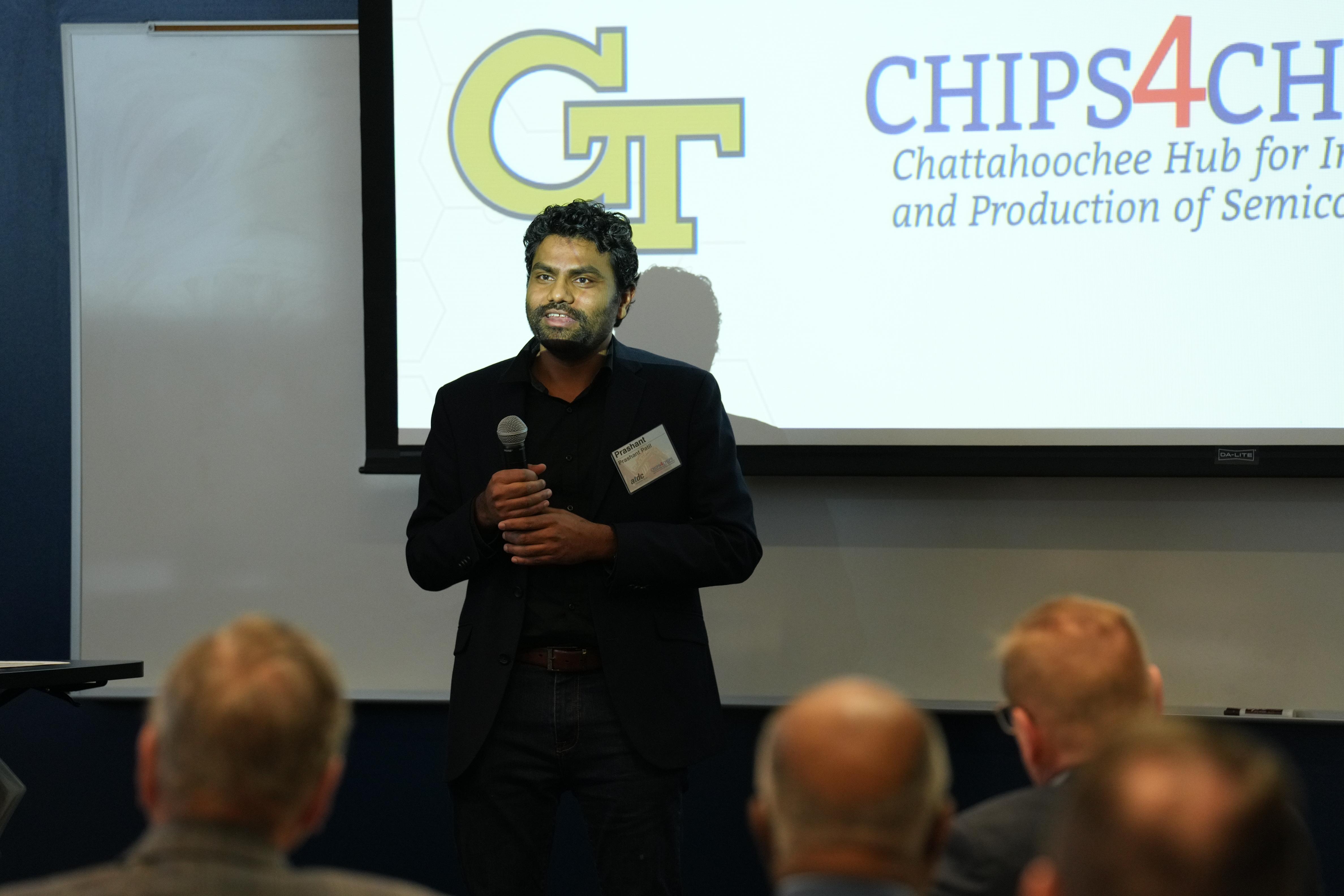
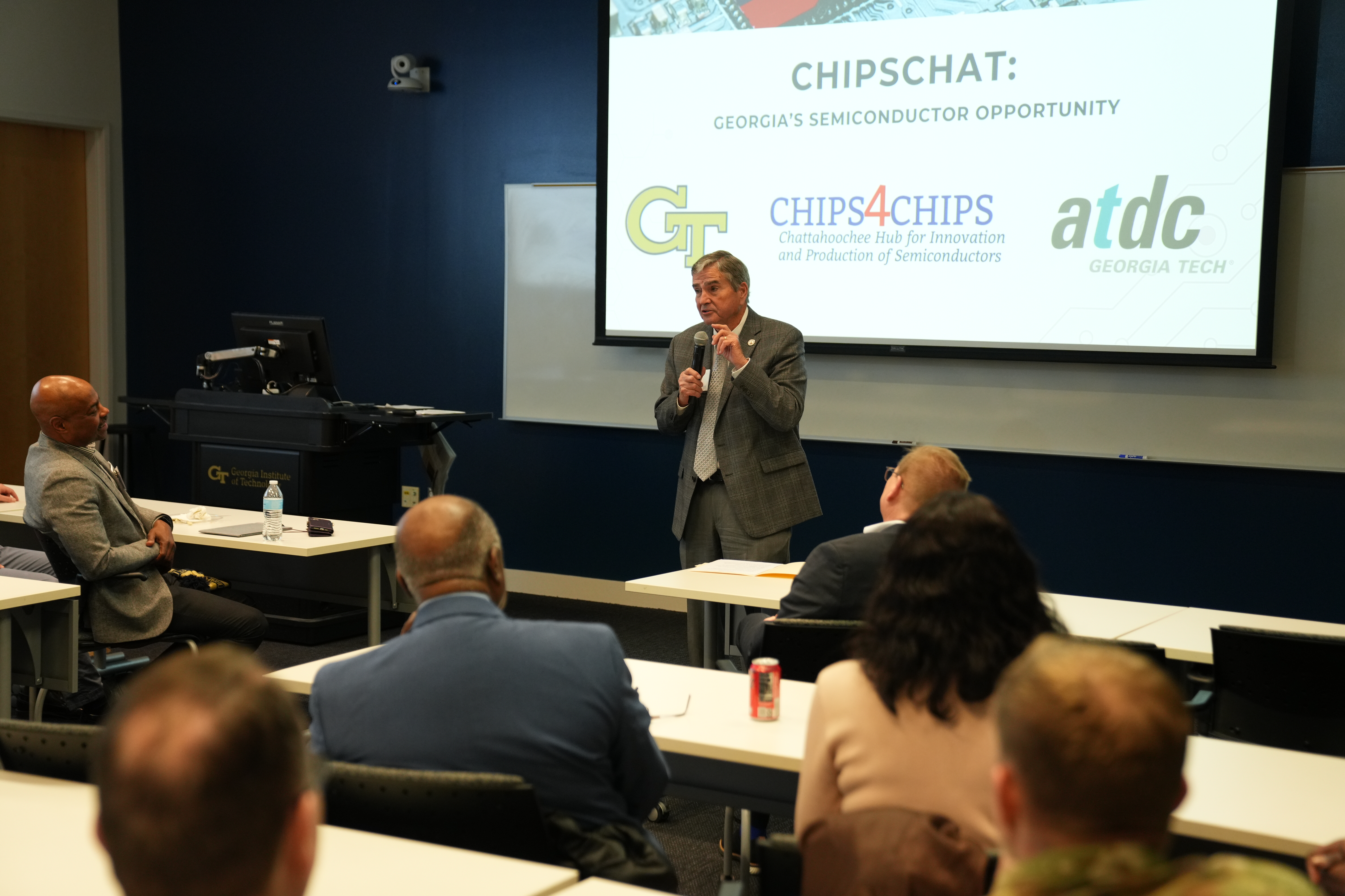
Prashant Patil, founder and CEO of Micromize, explains to a coalition of business, civic, and military stakeholders from Columbus, Georgia and Georgia Tech leaders why he opted to relocate his company to Columbus, Georgia from Massachusetts. (PHOTO: Chris Ruggiero)
The move is the result of strategic partnerships between Micromize, CHIPS4CHIPS (Chattahoochee Hub for Innovation and Production of Semiconductors/C4C), and several programs at Georgia Tech’s Enterprise Innovation Institute, including its Advanced Technology Development Center (ATDC), its Georgia Manufacturing Extension Partnership, and the Center for Economic Development Research. It also signifies a collaborative effort to harness the cutting-edge innovations in semiconductor packaging available at Tech’s Institute for Electronics and Nanotechnology.
"Our decision to locate in Columbus was driven by several crucial factors, and we are thrilled about the opportunities that this vibrant city presents for our growth and development,” said Prashant Patil, Micromize founder and CEO. “The work of CHIPS4CHIPS in supporting the semiconductor industry is commendable, and we are excited to be part of this innovative ecosystem.”
This exciting development was announced Tuesday, Jan. 23, at the Marcus Nanotechnology Center on Georgia Tech’s campus to a large group of state legislators and other state officials, a delegation of business and civic leaders from Columbus, and leadership from Georgia Tech and ATDC. The announcement is a true look at how statewide partnerships can lead to success for the Columbus region.
Micromize, a spinoff of the Massachusetts Institute of Technology, selected Georgia as its new home, in part, to take advantage of the semiconductor packaging expertise at Georgia Tech. The company plans to establish its headquarters and manufacturing facility in Columbus, further solidifying its presence in the state’s vibrant technology ecosystem. Additionally, Micromize will center its cutting-edge research and development on Georgia Tech's campus.
"The collaboration with Micromize is a significant milestone for CHIPS4CHIPS and the entire region,” said Ben Moser, president and CEO of United Way of the Chattahoochee Valley and chair of CHIPS4CHIPS. “This announcement marks the first of what we believe will be many to come, and we are thankful that Micromize recognizes the potential of our region for this industry. Columbus is poised for remarkable development, and we look forward to the positive impact that Micromize will bring to our community.”
The strategic relocation is expected to create significant economic opportunities in the region. Micromize will bring 20-25 jobs to Columbus through its headquarters and manufacturing facility, contributing to the local workforce, and fostering growth.
Micromize will center its Research & Development Lab at Georgia Tech’s 3D Systems Packaging Research Center, which is regarded as the world’s best for semiconductor packaging research. This partnership represents a synergistic collaboration of industry leaders, research institutions, and the entrepreneurial ecosystem. Micromize's move to Columbus not only underscores the city's growing prominence as a technology hub, but also highlights the collaborative efforts driving innovation and economic development in the state of Georgia.
In addition to C4C’s nationally recognized workforce development efforts, the Fort Moore Army base, and its skilled workforce, the region’s proximity to a port and airport will facilitate efficient shipping, and Columbus played a pivotal role in supporting the company by providing essential infrastructure, he said.
“Our collaboration with Georgia Tech enriches our talent pool, adds exponentially to our research and development capabilities, and access to mentorship at ATDC enhances our commercialization potential,” Patil said. “We are also proud to be part of the effort to revitalize semiconductor manufacturing in the United States, with Columbus serving as our starting point as we embark on this exciting journey of growth and innovation.”
Georgia Tech, a leader in microchips and nanotechnology research, innovation, and fabrication, provides fertile ground for Micromize's relocation. The Institute’s commitment to advancing semiconductor technology aligns with the national push at the federal level (via the CHIPS and Science Act) to bring more semiconductor production to the U.S., making it more competitive in research, development, and manufacturing.
“As the state’s technology startup incubator, we’re excited to welcome Micromize into our portfolio and to support them into the next phase of growth and expansion,” said ATDC Director John Avery.
“Microchips, semiconductor packaging, and microelectronics are critical to our national economy and national security. Micromize’s choosing Georgia as its home to grow reflects what is proving to be a successful model when business, government, and research institutions such as Georgia Tech collaborate.”
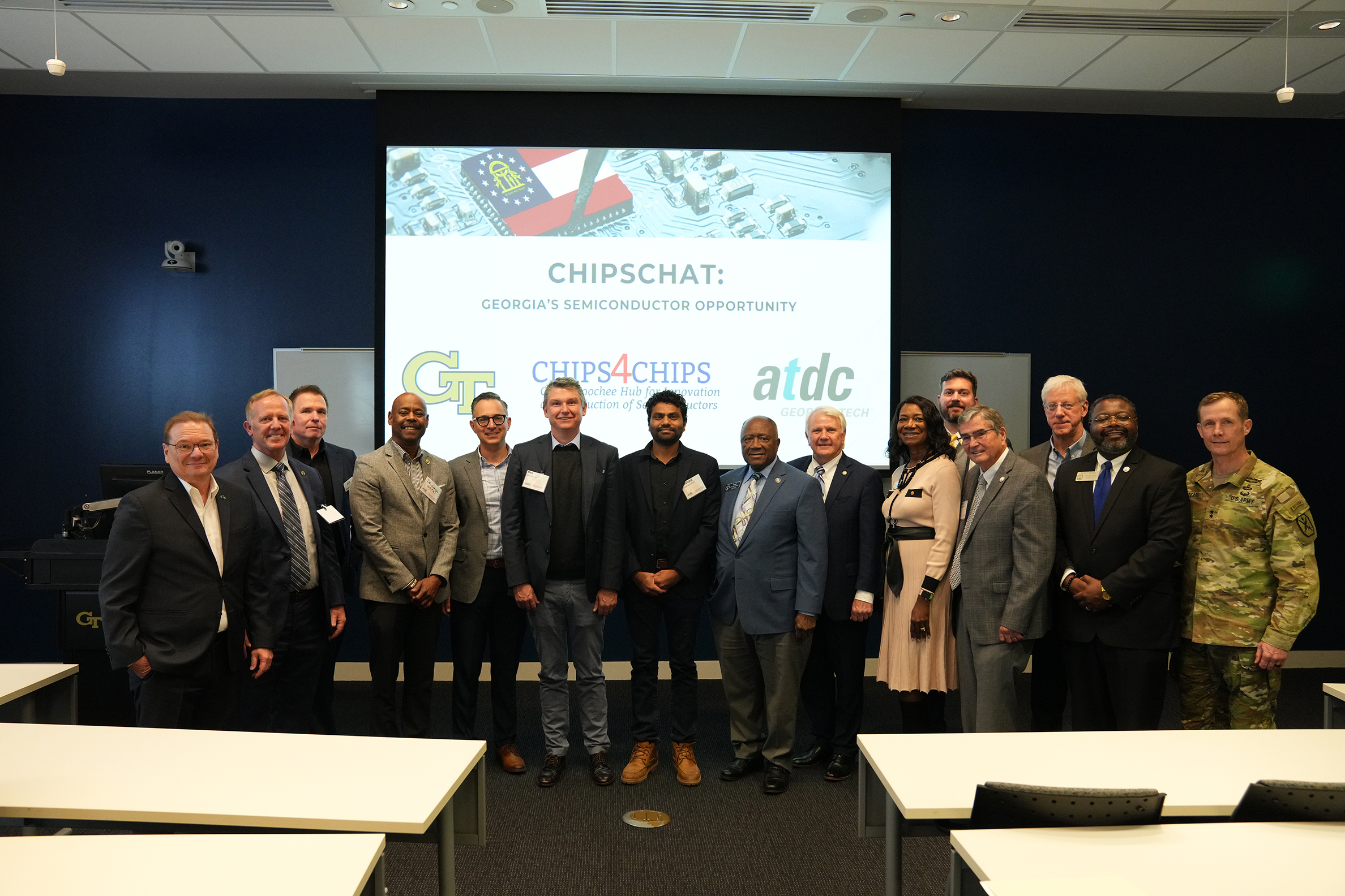
A coalition of business and civic leaders from Columbus, Georgia and several programs at Georgia Tech, including ATDC, announced Jan. 23, 2024, that semiconductor manufacturer, Micromize, is relocating to Georgia from Massachusetts. (PHOTO: Chris Ruggiero)
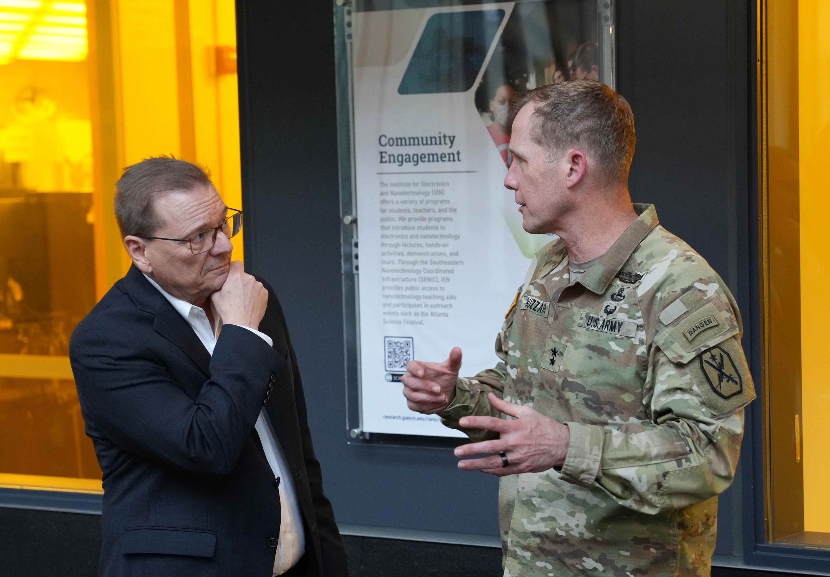
David Bridges, vice president of Georgia Tech's Enterprise Innovation Institute, speaks with Maj. Gen Curtis A. Buzzard, commanding general of the United States Army Maneuver Center of Excellence and Fort Moore in Columbus. Because of its skilled workforce, Fort Moore was one reason Micromize selected Georgia for its manufacturing facility. (PHOTO: Chris Ruggiero)
Georgia House Rep. Richard Smith, (R-Columbus), chairman of the Rules Committee, discusses how the collaboration that led to Micromize coming to Columbus could serve as a blueprint for more semiconductor companies developing in or moving to Georgia. (PHOTO: Chris Ruggiero)
Péralte C. Paul
404.316.1210
peralte@atdc.org
Some Georgia Tech researchers solve cosmic mysteries such as how supermassive black holes were born — and others now are getting a better, sharper look at those black holes.
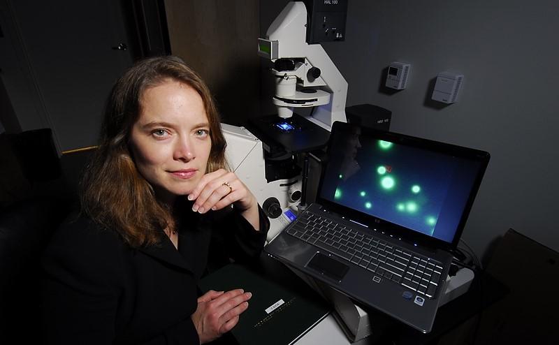
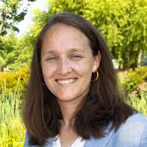
Valeria Tohver Milam leads the Macromolecular Materials at Biotic and Abiotic Interfaces research initiative for the Institute for Materials (IMat) and the Parker H. Petit Institute for Bioengineering and Biosciences at Georgia Tech. In this role, she is working to build an inclusive and active community across and beyond Georgia Tech to identify emerging research directions in macromolecular materials for biological and nonbiological applications. Milam is an associate professor in Materials Science and Engineering and a program faculty member of the Bioengineering graduate program at Georgia Tech.
In this brief Q&A, Milam discusses her research focus, how it relates to materials research, and the impact of this initiative.
What is your field of expertise and at what point in your life did you first become interested in this area?
My field of expertise lies in bio-inspired materials science and engineering. Natural macromolecular components of biological systems such as cell receptors or antibodies rely on recognition-based binding events to, for example, allow a cell to take up particular nutrients or to neutralize a specific pathogen threat. Inspired by nature’s capabilities, my group’s research strives to identify and study synthetic macromolecular materials with bio-inspired compositions and self-folded structures. I first became interested in using DNA for its recognition capabilities during my postdoc at the University of Pennsylvania. For the first several years as an assistant professor at Georgia Tech, my group used DNA duplexes as a temporary glue between particle surfaces. Our more recent efforts focus on finding oligonucleotides to function as ligands or capture agents for a specific biological or nonbiological target.
What questions or challenges sparked your current materials research?
Polymers or macromolecules hold a lot of promise as a class of materials for various applications. Synthetic macromolecules, however, pose a lot of synthesis and post-use challenges that can hinder the discovery and practical use of novel macromolecular chemistries. Natural polymers such as oligonucleotides and proteins, on the other hand, have their own elegant synthesis and degradation pathways. To promote discovery of novel macromolecular materials, my group uses nature’s reagents and building blocks to synthesize numerous artificial biopolymer candidates. Since we do not start with any sequence design rules, we rely on maximizing the composition diversity of these artificial biopolymers. We then test all candidates collectively to efficiently choose ones with the desired functionality.
Why is your initiative important to the development of Georgia Tech’s Materials research strategy?
One of the challenges to discovering macromolecular systems that are both novel and practical is the lack of design rules. For example, how does one choose the right number and composition of repeat units for a macromolecule that binds to a particular material surface or to a particular biological target. If you can take advantage of nature’s building blocks and enzymes, then you can explore a wide chemical combinatorial space without having to follow any prerequisite design rules. Better yet, you can then use your initial findings to come up with design rules to explore additional, possibly better macromolecular candidates. This approach to macromolecule discovery is inherently interdisciplinary since one must combine or adapt techniques and approaches developed by biologists, polymer scientists, and materials engineers. Thus, Georgia Tech is a great place to foster this interdisciplinary strategy to research.
What are the broader global and social benefits of the research you and your team conduct?
In addition to training members of our future workforce with interdisciplinary skill sets, we want to carve out a pathway to designing, synthesizing and using environmentally friendly, multiuse macromolecules with commercial promise.
What are your plans for engaging a wider GT faculty pool with IMat research?
Currently, we are primarily in the brainstorming stage. To this end, I am engaging with science and engineering faculty at GT as well as Emory. As cross-disciplinary ideas start to brew, we will work towards multi-PI funding opportunities that engage the broader GT faculty and community.
Amelia Neumeister
Research Communications