Nano@Tech Spring 2024 Series | Plenty of Room at the Top and Bottom

Abstract: Advances in the theory of semiconductors in the 1930s coupled with the purification of germanium and silicon crystals in the 1940s enabled the point-contact junction transistor demonstration in 1947 and initiated the era of semiconductor electronics. Gordon Moore postulated that the number of components in an integrated circuit would double every two years with associated reduction in cost per transistor. Transistor density doubling through “scaling” with each new process node continues today, albeit at a slower pace.

Researchers Create Faster and Cheaper Way to Print Tiny Metal Structures With Light

Two men stand in a lab

Assistant professor Sourabh Saha and Jungho Choi (Ph.D. student) in front of their superluminescent light projection system at Georgia Tech. Credit: Allison Carter

Researchers at the Georgia Institute of Technology have developed a light-based means of printing nano-sized metal structures that is significantly faster and cheaper than any technology currently available. It is a scalable solution that could transform a scientific field long reliant on technologies that are prohibitively expensive and slow. The breakthrough has the potential to bring new technologies out of labs and into the world.

Technological advances in many fields rely on the ability to print metallic structures that are nano-sized — a scale hundreds of times smaller than the width of a human hair. Sourabh Saha, assistant professor in the George W. Woodruff School of Mechanical Engineering, and Jungho Choi, a Ph.D. student in Saha’s lab, developed a technique for printing metal nanostructures that is 480 times faster and 35 times cheaper than the current conventional method.

Their research was published in the journal Advanced Materials.

Printing metal on the nanoscale — a technique known as nanopatterning — allows for the creation of unique structures with interesting functions. It is crucial for the development of many technologies, including electronic devices, solar energy conversion, sensors, and other systems.

It is generally believed that high-intensity light sources are required for nanoscale printing. But this type of tool, known as a femtosecond laser, can cost up to half a million dollars and is too expensive for most research labs and small businesses.

“As a scientific community, we don’t have the ability to make enough of these nanomaterials quickly and affordably, and that is why promising technologies often stay limited to the lab and don’t get translated into real-world applications,” Saha said.

“The question we wanted to answer is, ‘Do we really need a high-intensity femtosecond laser to print on the nanoscale?’ Our hypothesis was that we don’t need that light source to get the type of printing we want.”

They searched for a low-cost, low-intensity light that could be focused in a way similar to femtosecond lasers, and chose superluminescent light emitting diodes (SLEDs) for their commercial availability. SLEDs emit light that is a billion times less intense than that of femtosecond lasers.

Saha and Choi set out to create an original projection-style printing technology, designing a system that converts digital images into optical images and displays them on a glass surface. The system operates like digital projectors but produces images that are more sharply focused. They leveraged the unique properties of the superluminescent light to generate sharply focused images with minimal defects.

They then developed a clear ink solution made up of metal salt and added other chemicals to make sure the liquid could absorb light. When light from their projection system hit the solution, it caused a chemical reaction that converted the salt solution into metal. The metal nanoparticles stuck to the surface of the glass, and the agglomeration of the metal particles creates the nanostructures. Because it is a projection type of printing, it can print an entire structure in one go, rather than point by point — making it much faster.

After testing the technique, they found that projection-style nanoscale printing is possible even with low-intensity light, but only if the images are sharply focused. Saha and Choi believe that researchers can readily replicate their work using commercially available hardware. Unlike a pricey femtosecond laser, the type of SLED that Saha and Choi used in their printer costs about $3,000.

“At present, only top universities have access to these expensive technologies, and even then, they are located in shared facilities and are not always available,” Choi said. “We want to democratize the capability of nanoscale 3D printing, and we hope our research opens the door for greater access to this type of process at a low cost.”

The researchers say their technique will be particularly useful for people working in the fields of electronics, optics, and plasmonics, which all require a variety of complex metallic nanostructures.

“I think the metrics of cost and speed have been greatly undervalued in the scientific community that works on fabrication and manufacturing of tiny structures,” Saha said.

“In the real world, these metrics are important when it comes to translating discoveries from the lab to industry. Only when we have manufacturing techniques that take these metrics into account will we be able to fully leverage nanotechnology for societal benefit.”


Citation: J. Choi, S. K. Saha, Scalable Printing of Metal Nanostructures through Superluminescent Light Projection. Adv. Mater. 2024, 36, 2308112.

DOI: https://doi.org/10.1002/adma.202308112

Funding: Funding includes grants from the G.W.W. School of Mechanical Engineering and the EVPR’s office at the Georgia Institute of Technology. Imaging was performed at the Georgia Tech Institute for Electronics and Nanotechnology, a member of the National Nanotechnology Coordinated Infrastructure (NNCI), which is supported by the National Science Foundation (ECCS-2025462).

A gloved hand adjusts a dial on a piece of equipment

Ph.D. student Jungho Choi controlling LED brightness levels on the SLP system. Credit: Allison Carter

The Georgia Tech logo on a black background under a microscope

Scanning electron microscope image of a printed silver Georgia Tech logo made with the researchers' SLP technique. Credit: Jungho Choi

Two men in a lab and one of them is adjusting a piece of equipment

Choi (right) carries out optical adjustment for the correct focal plane of the SLP system. Credit: Allison Carter

 
News Contact

Catherine Barzler, Senior Research Writer/Editor

catherine.barzler@gatech.edu

Oliver Brand Memorial Technical Symposium

The Oliver Brand Memorial Technical Symposium is held in memory of the technical achievements of Professor Oliver Brand.

Speakers include members of the Microelectromechanical Systems (MEMS) research community at Georgia Tech who worked closely with Brand.

Agenda:

Nano@Tech Spring 2024 Series | Enabling Roll-to-Roll Manufacture of Thin Films through Conventional and Innovative Coating Processes

Abstract: In recent decades, printing and coating techniques have received interest for manufacturing of low-cost flexible electronics, membranes, electrochemical systems, packaging/encapsulation, and pharmaceuticals. The functionality of these devices and materials depends significantly on the print resolution, with typical feature sizes ranging from millimeters to microns and material properties with respect to scaled manufacture.

OPTEC Femtosecond Laser Micro-machining System Installation Presentation

The Optec LSV-Flex Micro-machining Laser System uses a femto-second laser to process practically any material through ultra-short laser pulse photo-ablation. The ultra-short laser pulse is effective on polymers, metal, glasses, single crystals, and polymorphic crystals. Materials are ionized by the laser pulse and removed from the surface in a plasma cloud, leaving a clean surface at the interaction site.

Georgia Tech Energy Materials Day

The Georgia Tech Energy Materials Day will bring together representatives from academia, government, and industry to accelerate energy materials research. It will also provide an opportunity for key stakeholders to interact with Georgia Tech researchers in this important area. 

Materials Research Science and Engineering Centers (MRSEC) Information Session

The National Science Foundation (NSF) is gearing up to unveil a major funding announcement in Fall 2024 to establish new Materials Research Science and Engineering Centers (MRSECs). These centers support interdisciplinary materials research and education addressing fundamental problems in science and engineering. MRSECs foster groundbreaking research and offer sustained support for university-based materials research. 

Six Named to National Academy of Inventors

Faculty selected for NIA

Six Georgia Tech College of Engineering faculty members are among the National Academy of Inventors (NAI) 2023 Class of Fellows. The honor is the highest professional distinction awarded solely to inventors.

No other university or organization in the world has more honorees this year than Georgia Tech. The group of six holds more than 200 patents.

  • Farrokh Ayazi, electrical and computer engineering
  • Maohong Fan, civil and environmental engineering
  • Christopher Jones, chemical and biomolecular engineering
  • Wilbur Lam, biomedical engineering
  • Susan Margulies, biomedical engineering
  • Karthikeyan Sundaresan, electrical and computer engineering

The Georgia Tech engineers are among 162 worldwide inventors honored in 2023. According to the NAI, “their work spans across disciplines and exemplifies their dedication and inspiration to translating research into commercial technologies that benefit society.”

The 2023 class will be honored in June at the NAI annual meeting.

Read the full story at the College of Engineering website.

 
News Contact

Jason Maderer, College of Engineering Director of Communications 


jason.maderer@coe.gatech.edu

Georgia Tech and Samsung Look to Unleash the Future of Digital Storage

Shot of Corridor in Working Data Center Full of Rack Servers and Supercomputers with Internet connection Visualisation Projection

The rise of artificial intelligent (AI)-driven marvels hinges on cutting-edge data storage solutions. Without efficient data storage, applications like self-driving cars, life-saving healthcare diagnostics, and responsive voice assistants would fall short of their true potential.

At the forefront of this evolving data storage landscape, a collaboration between the Georgia Institute of Technology and Samsung seeks to substantially decrease the voltage in existing technology, unlocking the full potential of AI systems.

“Finding innovative solutions in data storage is paramount, it’s not just about saving photos or documents anymore. The storage needed is about enabling AI systems to transform how we interact with our devices, the world around us, and even each other,” said Asif Khan, an assistant professor in the School of Electrical and Computer Engineering (ECE) with a joint appointment in the School of Materials Science and Engineering (MSE).

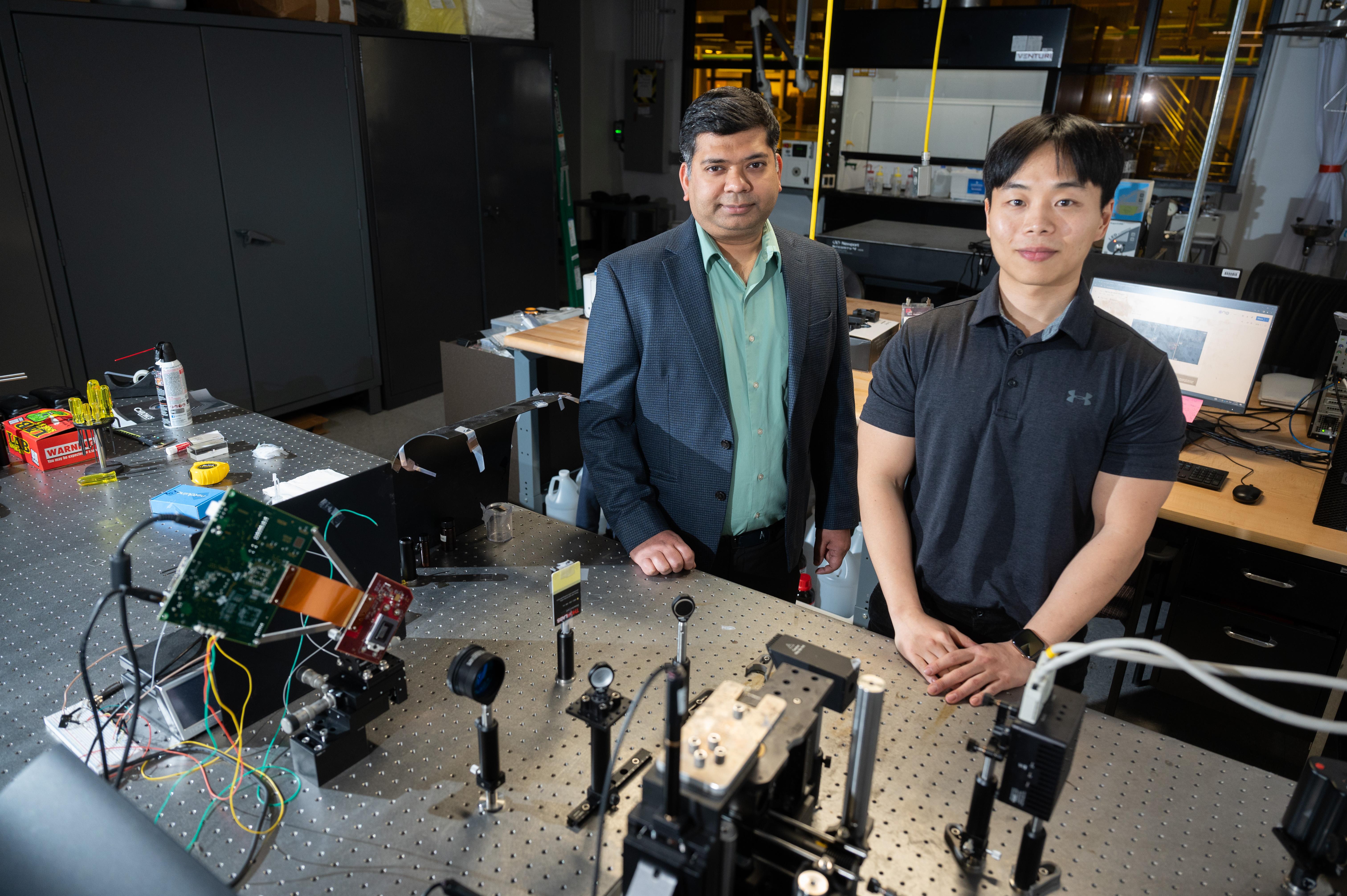
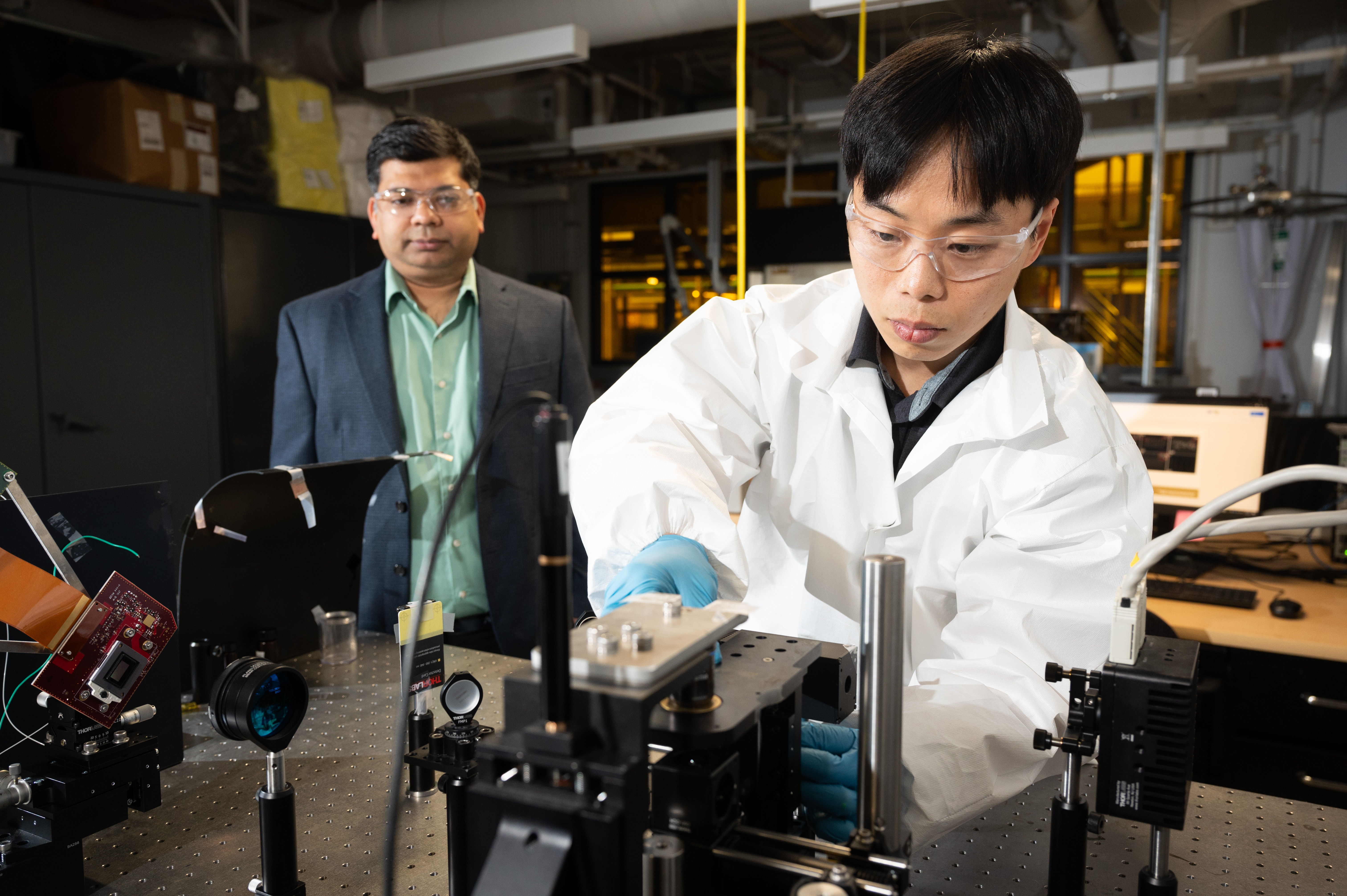
Khan's lab is spearheading the collaboration which brings together three ECE labs, including those of Professors Suman Datta and Shimeng Yu. The lead author of the paper is Dipjyoti Das, a postdoctoral fellow under Khan's supervision. The second author, Hyeonwoo Park, conducts research under Datta. The team is joined by researchers from MSE, the Institute of Materials, the Institute of Electronics and Nanotechnology, and a dedicated team from Samsung.

“This is a pivotal era of transformation and opportunity in high-memory compute,” said co-author Suhwan Lim, an engineer at Samsung. “Strategic intersectoral relationships like this between Samsung and Georgia Tech nurture innovative thinking and lead to exciting experiential results that push us all forward.”

Adding to the already substantial Georgia Tech presence in the field of computer memory storage, the team's findings will be featured at the upcoming International Electron Devices Meeting (IEDM) in San Francisco this month.

The Quest for Voltage Efficiency

The research focuses on improving NAND flash technology found at the core of storage devices like solid-state hard drives, USB sticks, and SD cards. NAND boasts an impressive 1,000-layer 3D architecture, cramming 100 terabytes of data into a minuscule space.

However, the critical challenge is NAND’s persistent high voltage requirements. Exceeding 20 volts poses challenges in computing due to increased energy consumption, heat generation, and the risk of damaging electronic components.

“NAND has been the backbone of data storage, so our research doesn't attempt to replace it; it's an upgrade. We're boosting NAND's power and pushing it into the digital storage future,” said Das, who designed and executed experiments, as well as contributed to characterization.

A Ferroelectric Future

The paper’s groundbreaking proposal aims to revolutionize NAND flash technology by replacing the traditional NAND gate stack — a multi-layered structure in a transistor essential for controlling the flow of electrical current in semiconductor devices — with a new ferroelectric structure and a tunneling barrier.

The team's method, introducing aluminum oxide (Al2O3) in the middle of the ferroelectric stack, has dramatically improved data storage capability, reducing voltage requirements by an impressive 40-60%.

Additionally, the study reveals that the Al2O3 layer functions as a tunnel barrier, impeding electron motion and establishing a dipole, creating an additional electric field that aligns with the polarization direction, boosting device memory performance.

The experiential findings could transform various sectors, including AI, mobile devices, edge data processing, embedded systems, and overall computing efficiency. 

“This breakthrough charts a new course towards more efficient, reliable and dense data storage solution,” said Datta, who is the Joseph M. Pettit Chair of Advanced Computing in ECE and a Georgia Research Alliance (GRA) Eminent Scholar. “We are grateful to Samsung for their continued support, as we work towards the next milestone.”

Looking for Collective Solutions to Shared Challenges

According to Das, the approach not only demonstrates the capability to achieve reduced voltage and enhanced memory but also aligns with scalability and broad industry adoption. 

As the project ventures into commercial avenues, the input of Samsung's researchers will be crucial. Das and Park are actively uncovering the intricacies of disturbances that could impede the market acceptance of the new gate stack.

In this context, disturbances refer to any unintended disruptions or deviations from transistor behavior expectations. Das stresses the importance of understanding, controlling, and clearly defining disturbance specifications. Establishing a well-defined threshold for disturbances is pivotal for achieving widespread commercialization readiness in their research.

“Working alongside industry leaders like Samsung is essential for any endeavor aiming to make a transformative impact in everyday technology,” added Khan. “It becomes particularly pertinent as we collectively look towards a future dominated by the power required to fuel advancements in AI.”
 

Citation: Dipjyoti Das*, Hyeonwoo Park*, Zekai Wang, Chengyang Zhang, Prasanna Venkatesan Ravindran, Chinsung Park, Nashrah Afroze, Po-Kai Hsu, Mengkun Tian, Hang Chen, Winston Chern, Suhwan Lim, Kwangsoo Kim, Kijoon Kim, Wanki Kim, Daewon Ha; Shimeng Yu, Suman Datta, Asif Khan. “Experimental Demonstration and Modeling of a Ferroelectric Gate Stack with a Tunnel Dielectric Insert for NAND Applications.” Proceedings of the 2023 IEEE International Electron Devices Meeting (IEDM). Paper # 24.1

 
News Contact

Dan Watson