
Cleanroom User Spotlight: Mason A. Chilmonczyk
May 25, 2022 — Atlanta, GA

Mason A. Chilmonczyk is the CEO and Co-founder of Andson Biotech, a startup that develops new sensors to discover the next groundbreaking cell and gene therapies. In the following Q&A, Chilmonczyk briefly discusses his work in the IEN cleanroom and gives advice to current and future users.
How long have you been using the IEN cleanroom?
I began using the IEN cleanroom eight years ago when I started my Ph.D. program at Georgia Tech and I am still using it today.
What tools have/do you use when you are in the cleanroom?
- Hitachi 4700 FE SEM
- SCS G3P8 Spinners
- Tystar Mini
- Vision RIE
- Unaxis RIE
- PlasmaTherm RIE
- PlasmaTherm ICP
- STS ICP
- Obducat Nanoimprinter
- ADT Dicing Saw
What is/has been your favorite project you have worked on in the IEN cleanroom?
My Ph.D. project, “The Dynamic Sampling Platform for Real-time Bioreactor Monitoring,” has been the most satisfying project I have worked on in the IEN cleanroom. I collaborated with my advisor, Mechanical Engineering Professor Andrei Fedorov, and we utilized the Nanoscribe to make micro-3d printed parts. This allowed me to take interesting SEM images using the Field Emissions Scanning Electron Microscopes. My Ph.D. project was probably the most satisfying to "complete," but I am still working on it to this day.
At the core of my work was a microfluidic mass exchanger that I built in the IEN cleanrooms at Georgia Tech. As a result of this project, Professor Fedorov and I co-founded the startup Andson Biotech. The company is growing, and we recently licensed the technology to enable better biopharmaceutical workflows.
What advice would you give to other researchers thinking about using a tool in the IEN cleanroom?
I would say to only use the cleanroom for your research if you have a burning desire to learn about MEMS/microfabrication or you have to do so for your project. There are very rarely "quick" projects inside cleanrooms. In general, I think if you have the opportunity to learn about anything new you should take that chance.
What is your favorite thing about the IEN cleanroom?
My favorite thing about the IEN cleanroom is the people I've met. Some of my best and longest-term friends have been made in these cleanrooms. I really miss working in the cleanroom as often as I used to, because I don't get to interact with all my best friends. Unfortunately, many of my original friends [from the cleanroom] have moved on to other things. While I miss seeing them, I love to see them succeed!
Learn more about Mason’s project, company, and technology - New Startup Makes Developing Gene Therapies Faster and Easier
Georgia Tech Faculty to Present Timely Topics at VLSI Symposium on Technology and Circuits
May 19, 2022 — Atlanta, GA

In June, some of the world’s top technologists in the VLSI (Very Large-Scale Integration) industry will convene in Honolulu for the 2022 IEEE Symposium on VLSI Technology and Circuits, one of the premier symposiums for microelectronics and semiconductor research. Now in its 42nd year, the VLSI Symposium offers attendees the opportunity to share and exchange ideas on the most relevant subjects in their fields and address current and future directions in the development of VLSI technology.
Given the continuing global semiconductor shortage, the theme of this year’s conference is “Technology and Circuits for the Critical Infrastructure of the Future.” Seven papers submitted by Georgia Tech faculty have been accepted and will be presented during the conference. Paper topics include Ferroelectric Memories, Resistive Memories, Embedded DRAM, and Power Converter based on GaN/Si. The contributing professors include Asif Khan, Arijit Raychowdhury, Shimeng Yu, and Suman Datta from Georgia Tech’s Institute of Electronics and Nanotechnology (IEN) and the School of Electrical and Computer Engineering (ECE).
In addition to presenting their papers, Datta and Yu are also organizing short courses on Monolithic and Heterogenous Integration and Advances in Application-Specific Computing Systems and Technologies. Muhannad Bakir will present on “2.5D and 3D Polylithic Integration Technologies” as part of the course on Monolithic and Heterogenous Integration.
“The VLSI Symposium is one of the most selective and prestigious venues to publish the latest advances in semiconductor technologies and circuits, and it has always had a strong industry presence,” said Raychowdhury, who also serves as the Steve W. Chaddick School Chair in ECE. “Our participation through multiple papers and invited talks is a clear testament of the depth and breadth of our research program. Congratulations to all of the students and faculty members who are making us proud through their impactful research.”
About the contributors:
Arijit Raychowdhury is the Steve W. Chaddick School Chair and Professor at ECE. His research interests include low power digital and mixed-signal circuit design, design of power converters, sensors and exploring interactions of circuits with device technologies. He holds more than 25 U.S. and international patents and has published over 80 articles in journals and refereed conferences. He holds a Ph.D. in electrical and computer engineering from Purdue University and a B.E. in electrical and telecommunication engineering from Jadavpur University in India.
Muhannad Bakir is the Dan Fielder Professor in ECE. His research interests include heterogeneous microsystem design and integration, including 2.5D and 3D ICs and packaging, advanced cooling and power delivery for emerging system architectures; electrical and photonic interconnect technologies; biosensor technologies and their integration with CMOS; and nanofabrication technologies. Bakir is an editor of IEEE Transactions on Electron Devices and an associate editor of IEEE Transactions on Components, Packaging and Manufacturing Technology.
Suman Datta will join the Georgia Tech faculty this fall as Joseph M. Pettit Chair in ECE and a Georgia Research Alliance (GRA) Eminent Scholar. He will also have a joint appointment with the School of Materials Science and Engineering (MSE). His research involves high-performance, heterogenous computing, brain-inspired computing, and collective state computing using advanced CMOS (complementary metal–oxide–semiconductor) and beyond-CMOS devices. He also focuses on the development of semiconductor technologies for other types of computing, including intermittent computing, cryogenic computing, and harsh environment computing.
Asif Khan is an assistant professor in ECE with a courtesy appointment in MSE. His research focuses on microelectronic devices, specifically on ferroelectric devices that address the challenges faced by the semiconductor industry due to the end of transistor miniaturization. His research group at Georgia Tech focuses on all aspects of ferroelectricity ranging from materials physics, growth, and electron microscopy to micro- and nano-fabrication of electronic devices, all the way to ferroelectric circuits and systems for artificial intelligence, machine learning, and data-centric applications.
Shimeng Yu is an associate professor in ECE. He has both a master’s and Ph.D. in electrical engineering from Stanford University and a B.S. in microelectronics from Peking University. His research interests lie in nanoelectronic devices and circuits for energy-efficient computing systems. His expertise is on the emerging non-volatile memories (e.g., RRAM, ferroelectrics) for different applications such as deep learning accelerator, neuromorphic computing, monolithic 3D integration, and hardware security.
The IEEE Symposium on VLSI Technology and Circuits is a five-day hybrid event known as the microelectronics industry’s premiere international conference integrating technology, circuits, and systems with a range and scope unlike any other conference. In addition to the technical presentations, the Symposium program will feature a demonstration session, evening panel discussions, joint focus sessions, short courses, workshops, and a special forum session that provides a focused discussion on a specific topic relevant to the Symposia theme. To learn more visit http://www.vlsisymposium.org.
Spring 2022 IEN Seed Grant Winners Announced
May 17, 2022 — Atlanta, GA

The Institute for Electronics and Nanotechnology (IEN) at Georgia Tech has announced the winners for the 2022 Spring Core Facility Seed Grants. The primary purpose of this program is to give first- and second-year graduate students in diverse disciplines working on original and unfunded research in micro- and nano-scale projects the opportunity to access the most advanced academic cleanroom space in the Southeast. In addition to accessing the high-level fabrication, lithography, and characterization tools in the labs, the awardees will have the opportunity to gain proficiency in cleanroom and tool methodology and access the consultation services provided by research staff members in IEN. Seed Grant awardees are also provided travel support to present their research at a scientific conference.
In addition to student research skill development, this bi-annual grant program gives faculty with novel research topics the ability to develop preliminary data to pursue follow-up funding sources. The Core Facility Seed Grant program is supported by the Southeastern Nanotechnology Infrastructure Corridor (SENIC), a member of the National Science Foundation’s National Nanotechnology Coordinated Infrastructure (NNCI).
Since the start of the grant program in 2014, 78 projects from ten different schools in Georgia Tech’s Colleges of Engineering and Science, as well as the Georgia Tech Research Institute and three other universities, have been seeded.
The six winning projects in this round were awarded IEN cleanroom and lab access time to be used over the next year. In keeping with the interdisciplinary mission of IEN, the projects that will be enabled by the grants include research in semiconductor technology, metamaterials, quantum devices, polymer films, and materials analysis.
The Spring 2022 IEN Core Facility Seed Grant Award winners are:
Customized Nonlinear Metamaterials for Photon Upconversion
PI: Wenshan Cai | Student: Anjan Goswami
School of Electrical and Computer Engineering/School of Materials Science and Engineering
Fabricating Semiconductor Moiré Quantum Devices for Quantum Information Applications
PI: Zhigang Jiang | Student: Wei-Chen Wang
School of Physics
Enhancing Ferroelectric Switching Through Sputter Process Control in AlScN
PI: Lauren Garten | Student: John Wellington-Johnson
School of Materials Science and Engineering
Self-Repairing Polymeric Films as Artificial Solid-Electrolyte Interface Enabling Rechargeable Zinc Metal Batteries
PI: Seung Woo Lee | Student: Kun Ryu
George W. Woodruff School of Mechanical Engineering
New Applications of Raman Spectroscopy for Determining Sediment Provenance in the Southern Alps of New Zealand
PI: Karl Lang | Student: Dru-Ann Harris
School of Earth and Atmospheric Sciences
Next-generation Back-illuminated Silicon Photomultipliers with Multi-layer Antireflection Coatings on Textured Surface
PIs: Anna Erickson and Yuguo Tao | Student: Mackenzie Duce
George W. Woodruff School of Mechanical Engineering (Nuclear and Radiological Engineering Program)
The Southeastern Nanotechnology Infrastructure Corridor (SENIC), a member of the National Nanotechnology Coordinated Infrastructure (NNCI), is funded by NSF Grant ECCS-2025462.
Georgia Tech Researchers Develop Wireless Implantable Vascular Monitoring System
May 12, 2022 — Atlanta, GA

Woon-Hong Yeo and his research team have developed a new wireless, electronic vascular monitoring system - a smart stent.
Vascular diseases are public enemy number one: the leading killers worldwide, accounting for nearly a third of all human deaths on the planet.
Continuous monitoring of hemodynamics – blood flow through the vascular system – can improve treatments and patient outcomes. But deadly conditions like hypertension and atherosclerosis occur in long and twisting vascular system with arteries of varying diameter and curvature, and existing clinical devices are limited by their bulk, rigidity, and utility.
Georgia Institute of Technology researcher Woon-Hong Yeo and his collaborators are trying to improve the odds for patients with development of an implantable soft electronic monitoring system. Their new device, consisting of a smart stent and printed soft sensors, is capable of wireless real-time monitoring of hemodynamics without batteries or circuits.
“This electronic system is designed to wirelessly deliver hemodynamic data, including arterial pressure, pulse, and flow, to an external data acquisition system, and it is super small and thin, which is why we can use a catheter to deliver it, anywhere inside the body,” said Yeo, whose team released its study this week in the journal Science Advances.
Yeo added, smiling, “It’s like a stent with multiple tricks up its sleeve.”
For example, when this device is installed in a patient with atherosclerosis, in addition to expanding and preventing the artery from narrowing, like a traditional stent, restoring normal blood flow, it will also provide a constant flow of data.
“Now, once you have deployed a stent, you’re not sure if the problem was resolved and patients may come back with the same issue,” Yeo said. “It can be a defect of the stent, or an issue with stent deployment, or perhaps a problem with the patient’s blood flow.”
And the current standard way to monitor all of that is with an angiogram. That can be expensive and in rare instances, particularly with patients also struggling with diabetes, the dyes and radiation used in angiogram imaging can cause cancer. Yeo’s system seeks to circumvent the need for an angiogram or other imaging requirements.
His wireless smart stent platform, integrated with soft sensors, is operated by inductive coupling to offer wireless real-time monitoring that can detect a wide range of vascular conditions. Inductive coupling uses magnetic fields for wireless energy transfer. It’s similar to what’s happening when you use a wireless charger for your phone, smartwatch, or other devices – they are gaining energy from the magnetic field created by the charger.
“Basically, you can put this sensor system anywhere inside the body,” Yeo explained. “The other thing about this technology platform is, in addition to being an implantable sensor system, it can be used as a wearable system. Think about a smartwatch and how much of its bulk is taken up by circuits or batteries. If you remove all of that, you have a device that is thinner than a typical Band-Aid, an almost invisible health monitor that you can wear anywhere.”
That’s the long-range goal, anyway. So far, they’ve tested their wireless implantable system on animal models. However, there is still plenty of work to do. And Yeo also has the backing of the National Science Foundation to advance the technology. He recently received a 3-year, $400,000 grant from NSF focused on his printed nanomembrane sensors and bioelectronics for wireless and continuous monitoring of vascular health.
“We believe that the mechanical, material, and electrical design principles we develop, and the engineering and biosensing framework that results from this work, will advance the field of implantable electronics and biomedical systems,” Yeo said. “And the insights and knowledge we gain will be applicable for other physiological processes and challenges in biomedical science and engineering.”
CITATION: Robert Herbert, Hyo-Ryoung Lim, Bruno Rigo, Woon-Hong Yeo. "Fully implantable wireless batteryless vascular electronics with printed soft sensors for multiplex sensing of hemodynamics." Science Advances (May 2022)
COMPETING INTERESTS: Hyo-Ryoung and Yeo are the inventors for a pending U.S. patent application related to the work described here. The authors declare that they have no other competing interests.
FUNDING: American Heart Association (grant 19IPLOI34760577), National Institutes of Health (NIH R03EB028928).
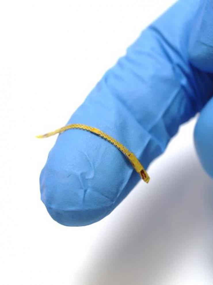
This smart stent can continuously monitor arterial pressure, pulse, and flow.
Center for Advanced Electronics through Machine Learning Receives Phase II Funding from The National Science Foundation
May 09, 2022 — Atlanta, GA

Madhavan Swaminathan
As the global demand for microelectronics continues to surge, the mission of the Center for Advanced Electronics through Machine Learning (CAEML) to “apply machine learning to the design of optimized microelectronic circuits and systems” has become even more crucial. As part of Phase I funding from the National Science Foundation (NSF), CAEML researchers and students worked closely with industry partners to develop models and design tools to enable efficient and reliable fabrication of microelectronic systems while protecting intellectual property. With the new Phase II funding, this effort is expected to grow significantly through increased interest and partnership from the semiconductor industry.
“Design space exploration and optimization have had limited success in the past due to slow simulators,” said Madhavan Swaminathan, CAEML site director at Georgia Tech. “In Phase I we have repeatedly shown that machine learning based methods can significantly improve computational time and enhance productivity. These advantages have been quantified by several CAEML industry partners through deployment of these techniques into their workflow.”
During phase I, the team published more than 70 papers, delivered 20 webinars, and received 11 awards or award nominations for their work with the Center. In addition, 12 students who participated in CAEML’s Phase I research have been hired by industry partners.
CAEML is part of the NSF’s Industry-University Cooperative Research Center (IUCRC) program and includes faculty from Georgia Tech, the University of Illinois Urbana-Champaign (UIUC), and North Carolina State University (NCSU). Phase II is a five-year award and begins August 1, 2022.
“In Phase II we plan to address the end-to-end system design challenges by developing solutions to five technical challenges posed by industry using machine learning in the areas of analog circuit design, signal integrity, hardware security, reliability, and data access,” said Swaminathan, who also serves as the John Pippin Chair in Microsystems Packaging and Electromagnetics and Director of the Packaging Research Center at Georgia Tech.
In addition to Swaminathan, the leadership team for CAEML consists of Elyse Rosenbaum, Melvin and Anne Louise Hassebrock Professor in Electrical and Computer Engineering, UIUC and Paul Franzon, Cirrus Logic Distinguished Professor of Electrical and Computer Engineering and Director of Graduate Programs in Electrical and Computer Engineering at NCSU.
Read the full press release.
NNCI Webinar: Societal and Ethical Implications
Science Policy Around the World in 2022: Innovations and Uncertainties in the Global Knowledge System
During the last two years, we have been living in a foreign world. Most activities have been altered in response to the Covid-19 pandemic, shifting our ways of living and interaction with others. Even the mechanisms through which we gather knowledge have changed.
Paul Joseph Awarded Fulbright Specialist Grant to India
Apr 29, 2022 — Atlanta, GA

Paul Joseph, a principal research scientist in the Institute for Electronics and Nanotechnology (IEN) at Georgia Tech, has received a Fulbright Specialist Award to India from the Fulbright Foreign Scholarship Board. Joseph will spend two weeks at the Indian Institute of Information technology (IIIT) this summer helping to expand the nanotechnology curriculum and assisting with faculty and student skill development at IIIT.
Joseph will bring more than 25 years of research and teaching experience in an academic setting to his host institution. In his current role at IEN, Joseph serves as the director of external user programs for the Southeastern Nanotechnology Infrastructure Corridor (SENIC) and manages and facilitates external research projects for academic and industry users of the NSF-funded National Nanotechnology Coordinated Infrastructure (NNCI) shared user labs. He also teaches a short course in soft lithography for microfluidics, coordinates the NanoFANS Forum, and conducts collaborative research with other faculty colleagues at Georgia Tech in micro- and nanotechnology.
Recently, Joseph received his MBA specializing in technology innovation and commercialization from the Scheller College of Business at Georgia Tech. He was also elected as IEN’s representative to the Georgia Tech Interdisciplinary Research Faculty Advisory Council. He plans to share his knowledge, specifically in nano- and microelectronics, fabrication methodologies, and nanomaterial characterization, through lectures and daily mentoring hours for IIIT students.
“My lectures on important topics will expose the students to the benefits of nanotechnology and will help widen their knowledge and skills in the field,” explained Joseph. “I hope this will help them explore career opportunities in nanoscale science and technology, which are expanding rapidly due to their increasing impact on many aspects of our daily lives.
“Nanotechnology offers the potential for tremendous advancements in the development of commercial products in electronics, energy, healthcare, the environment, and food, just to name a few,” he added. “It is one of the most powerful emerging and enabling technologies in the world, and Indian industries have started realizing the commercial viability of nanotechnology quite recently. Because of this, it is one of the hottest career options available to Indian engineering/science graduates.”
Joseph also hopes to create lasting relationships with the faculty at IIIT that will last beyond this visit. He plans to conduct group lectures and discussion sessions with faculty members on student engagement, course design for transformative education, best practices to gain research funding, how to design and lead a collaborative research team, and technology commercialization assessments for potential start-ups.
Beyond the benefits to Georgia Tech and IIIT, Joseph, who is a native of India, expects to benefit personally as well. “I see this as a great opportunity to participate in cross-cultural professional development, gain international exposure, and use my many years of experience in a new and a creative way,” he said. “It is a great opportunity to share my expertise and life experiences with overseas counterparts and learn about my field of research from a new perspective. I am very excited for this opportunity to give back to the country where I was born.”
IEN’s NanoFANS Forum Celebrates 25th Symposium
Apr 29, 2022 — Atlanta, GA

The NanoFANS (Focusing on Advanced Nanobio Systems) Forum is a semiannual symposium supported by the Institute for Electronics and Nanotechnology (IEN) at Georgia Tech that began in 2008. It features topics at the intersection of the life sciences and nanotechnology, and connects the medical, life sciences, biology, nanotechnology, and engineering communities. The goal of the NanoFANS Forum is to engage researchers in the biomedical and life sciences areas and to educate them on the benefits of micro-/nanotechnology and how it can advance their research.
Since the beginning, NanoFANS has been attended by more than 2,500 participants, both on- and off-campus, from academia, industry, and government organizations. To date, IEN has hosted 24 events and featured about 80 Georgia Tech / Emory faculty (and one off-campus faculty from Clemson).
The 25th NanoFANS forum is on Tuesday, May 24th, and will focus on “Micro- and Nanotechnology Commercialization: Opportunities and Challenges.” Technology commercialization is the process of transitioning technologies from the research lab to the marketplace, and it complements the process of publishing research findings. Innovations in micro- and nanotechnology are revolutionizing manufacturing and production and creating new materials and products through novel processes for commercial applications. In many cases, there is also a significant benefit to society.
IEN’s 25th NanoFANS forum will explore the opportunities and challenges of commercializing innovations in micro- / nanotechnology in the bio- space. Speakers will include Professor Todd Sulchek from the Woodruff School of Mechanical Engineering at Georgia Tech; Professor Farrokh Ayazi from the School of Electrical and Computer Engineer at Georgia Tech, Regents Professor Mark Prausnitz from the School of Chemical and Biomolecular Engineering at Georgia Tech, and Mason Chilmonczyk, CEO of Andson Biotech. They will discuss their innovations and commercialization experience as founders and co-founders of their start-ups.
Please register for the NanoFANS Forum by May 20, 2022. Lunch will be provided
After the talks, an optional tour of the state-of-the-art IEN Cleanrooms and labs will be available for interested participants. Please let us know if you are interested in taking a tour.
For more information on the NanoFANS Forum, please contact:
Paul J. Joseph, Ph.D., MBA
Principal Research Scientist
Georgia Tech Institute for Electronics and Nanotechnology
Spring 2022 IEN Microfabrication Short Course
The Institute for Electronics and Nanotechnology (IEN) at Georgia Tech will offer a short course on microfabrication from May 25th - 27th, 2022. This intensive three-day short course combines classroom lectures and laboratory based hands-on fabrication in the IEN cleanroom. The goal of the course is to impart a basic understanding of the science and technology of microfabrication processes as used in academia and industry.
PRC Distinguished Lecture Seminar | Directions in III-N Devices for Wireless Communications and Beyond
Featuring Professor Patrick Fay, Department of Electrical Engineering, University of Notre Dame