Nano@Tech Fall 2022 Series | Integrated Photonics
Integrated Photonics
Featuring Stephen Ralph | School of Electrical and Computer Engineering at Georgia Tech
Nano@Tech Fall 2022 Series | Thermally Responsive Materials for Clean Water and Energy
Thermally Responsive Materials for Clean Water and Energy
Featuring Akanksha Menon | School of Mechanical Engineering, Georgia Tech
Nano@Tech Fall 2022 Series | Ultrasound for Brain Imaging and Therapy
Ultrasound for Brain Imaging and Therapy
Featuring Chengzhi Shi | School of Mechanical Engineering, Georgia Institute of Technology
Nano@Tech Fall 2022 Series | Biomimetic Scaffolds for Tissue Repair and Regeneration
Biomimetic Scaffolds for Tissue Repair and Regeneration
Featuring Younan Xia | School of Biomedical Engineering at Georgia Tech and Emory University
Nano@Tech Fall 2022 Series | Next-Generation Vertical GaN Power Devices Using Selective-Area Doping Techniques
Next-Generation Vertical GaN Power Devices Using Selective-Area Doping Techniques
Featuring Spyros Pavlidis | School of Electrical and Computer Engineering, NC State University
Natalie Stingelin selected as new chair of MSE
Jun 17, 2022 — Atlanta, GA

Natalie Stingelin has been selected as the next chair of the School of Materials Science and Engineering (MSE) at the Georgia Institute of Technology. Stingelin has been a faculty member in the College of Engineering since 2016, with joint appointments in MSE and the School of Chemical and Biomolecular Engineering. She will begin her new role August 1.
“Natalie is an innovator with a bold vision for the future. These attributes, in addition to being a world-renowned researcher and her ongoing efforts to increase diversity in engineering, make her the best choice to lead MSE,” said Raheem Beyah, dean of the College of Engineering and Southern Company Chair. “I’m excited to continue to partner with Natalie as she begins this new chapter of her Georgia Tech career.”
Stingelin is a well-regarded researcher in polymer physics, functional soft matter, organic electronics and photonics, and bioelectronics. She received the 2022 Georgia Tech Outstanding Achievement in Research Innovation Award. She serves as the director of Georgia Tech’s Center for Organic Photonics and Electronics and is an initiative lead for the Institute for Materials.
“I am honored to have the opportunity to serve as the next chair of the School of Materials Science and Engineering,” Stingelin said. “I am very much looking forward to working closely with our students, faculty, and staff to foster and nurture an inclusive and impactful MSE community. I’m also excited to promote the School’s excellence in delivering transformational science and engineering, strengthening ties across campus with the other Schools and Colleges, and helping to revolutionize materials science education as we embrace the increasingly multidisciplinary nature of our field.”
Stingelin is a fellow of the Materials Research Society and the UK’s Royal Society of Chemistry. In 2021, she was elected a Fellow of the National Academy of Inventors (NAI), an honor given to the highest level of academic inventors. The NAI recognized Stingelin’s significant contributions in polymer physics and organic electronics and photonics. This includes the advancement of novel strategies, like organic semiconductors and inorganic/organic hybrid materials, that enable processing and design of soft electronics with unique functional properties as well as her work creating innovative device architectures.
In 2021, she was selected for the French-British Prize by the French Society of Chemistry and the U.K.'s Royal Society of Chemistry. The same year, she also received a prestigious Suffrage Science award for the Engineering and Physical Sciences. She was one of 12 women chosen by their peers for outstanding scientific research, communication work, and support of women in STEM
Stingelin was awarded a Chaire Internationale Associée by the Excellence Initiative of the Université de Bordeaux in 2017, and she won the Institute of Materials, Minerals & Mining's Rosenhain Medal and Prize in 2014.
Stingelin’s career has included six years at the Imperial College London, as well as positions at the Philips Research Laboratories in the Netherlands and the University of Cambridge.
She succeeds Naresh Thadhani, who is stepping down as chair after 10 years and returning to the faculty. Since MSE was formed in 2010, the School has been consistently ranked among the top materials programs in the nation by U.S. News & World Report. The program is ranked fourth among undergraduate programs and seventh among graduate programs.
“I’m thankful for Naresh’s leadership and guidance in MSE. He has been instrumental in building a young program into a national leader,” Beyah said. “I’m also grateful to the MSE search advisory committee, which was led by Krista Walton and included faculty, staff, and students. This group identified and interviewed a diverse pool of candidates and ensured that MSE and its leadership team will have a seamless transition as we begin the fall semester.”
Researchers Develop Wideband Millimeter Wave Transmit/Receive Module
Jun 15, 2022 — Atlanta, GA

GTRI researcher Paul Jo checks an RF test board with FCBGA packaged single-channel T/R module chips. (Credit: Sean McNeil, GTRI)
Researchers at the Georgia Institute of Technology are developing a wideband four-channel millimeter wave transmit-receive (T/R) module based on silicon-germanium (SiGe) technology that will support active electronically-scanned arrays (AESA) for potential military applications.
Designed to operate between 18 GHz and 50 GHz, the module could help address threat systems operating at millimeter wave frequencies and provide to military applications many of the advantages that millimeter wave technology is bringing to commercial applications such as 5G wireless, internet-of-things devices, and radar-based vehicle collision avoidance systems.
“The goal is to demonstrate small size, weight, power, and cost in a wideband millimeter wave T/R module,” said Paul Jo, a Georgia Tech Research Institute (GTRI) research engineer who is leading the project. “This would be a major module at the front of the AESA system, right behind the radiator element to process signals.”
Known as Millimeter Wave Active Electronically Scanned Array using Silicon-Germanium Transmit/Receive Modules (MAESTRO), the project represents a collaboration of GTRI and SiGe specialists in Georgia Tech’s School of Electrical and Computer Engineering. The use of SiGe helps support the high level of integration necessary for the miniaturization required by the module’s high-frequency operation.
“When it comes to millimeter wave frequencies, the AESA element lattice is less than one centimeter in size, and at 50 GHz, it’s three millimeters, which is very challenging to work with,” Jo noted. “That forces an extreme level of integration and miniaturization for this T/R system, which we are addressing through design and fabrication of the small SiGe monolithic microwave integrated circuit (MMIC) die.”
The researchers recently completed the fabrication and packaging of a core channel T/R module die, and are designing an evaluation board to demonstrate performance of the module. Also completed is the fabrication of a stand-alone radiator board for wideband and high-frequency applications; that evaluation board also is under test.
Wideband AESAs are an enabling technology for current and future military radar and communications systems by providing rapid beam steering, graceful degradation, electronic production, and low probability of intercept. The atmospheric attenuation of radio-frequency (RF) signals at millimeter wave frequencies is much greater than at microwave frequencies. As a result, high-gain directional apertures such as AESAs are required to propagate energy over tactically relevant distances.
Beyond the high level of integration, the system presents technical challenges related to manufacturing, packaging, and thermal management. For packaging MAESTRO, the research team is evaluating a Flip-Chip Ball Grid Array (FCBGA) solution to reduce the signal path from the die to the printed circuit board.
Earlier in the four-year project, the research team designed and fabricated single-channel and four-channel T/R modules and measured the RF performance of a chip-on-board (CoB)-assembled single-channel T/R module. The measured results confirmed that the designed digital control circuitry works for both Tx and Rx modes – attenuation and true-time delay – and that the time delay was consistent across the target bandwidth.
The MAESTRO program is a collaboration between GTRI and the research team of John Cressler, a Regents Professor at the Georgia Tech School of Electrical and Computer Engineering. Cressler’s team specializes in SiGe for heterojunction bipolar devices designed to provide high-frequency performance in mixed-signal circuit and analog circuit ICs.
“Silicon is a standard technology that industry is using to integrate very complicated systems,” Jo noted. “Since we needed to integrate the whole T/R module system into a very small lattice spacing, we decided to use SiGe to integrate all the discrete components.”
During testing of the T/R module, the researchers realized that the receive mode of their system could operate at even lower frequencies – down to 5 GHz – giving it an operating range of 5 GHz to 50 GHz. Efforts are underway to expand the range of the transmit mode to accommodate a similarly wider frequency band.
The MAESTRO project is part of a GTRI initiative to use SiGe semiconductor technology for a variety of RF applications. The SiGe Multifunction IC for Radio Frequency (SMIRF) program is developing a wideband, multichannel, reconfigurable radio frequency transceiver integrated circuit using the SiGe technology. The goal is to enable element-level digital beamforming of an AESA for RF-converged multifunction systems to support concurrent operating modes such as radar, communications, electronic warfare, positioning, and signals intelligence (SIGINT).
MAESTRO has been supported by GTRI’s Independent Research and Development program.
Writer: John Toon (John.Toon@gtri.gatech.edu)
GTRI Communications
Georgia Tech Research Institute
Atlanta, Georgia USA
The Georgia Tech Research Institute (GTRI) is the nonprofit, applied research division of the Georgia Institute of Technology (Georgia Tech). Founded in 1934 as the Engineering Experiment Station, GTRI has grown to more than 2,800 employees, supporting eight laboratories in over 20 locations around the country and performing more than $700 million of problem-solving research annually for government and industry. GTRI's renowned researchers combine science, engineering, economics, policy, and technical expertise to solve complex problems for the U.S. federal government, state, and industry.
 quad-channel T/R module")
Image shows a bare die (left) and fully packaged flip-chip ball grid array (FCBGA) quad-channel T/R module. (Credit: Sean McNeil, GTRI)
(Interim) Director of Communications
Michelle Gowdy
Michelle.Gowdy@gtri.gatech.edu
404-407-8060
Krishna Inducted into HPCA Hall of Fame
Jun 06, 2022 — Atlanta, GA
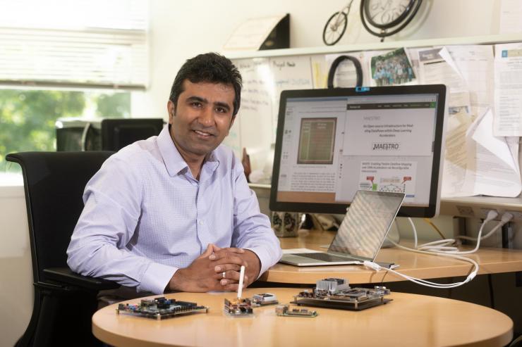
The research of Assistant Professor Tushar Krishna focuses on building hardware platforms to run AI applications efficiently. (Photo: Allison Carter, Georgia Tech)
With his eighth and ninth papers published in this year’s IEEE International Symposium on High-Performance Computer Architecture (HPCA), Tushar Krishna has been inducted into the organization’s Hall of Fame. Only 10 members of the HPCA community were inducted to the Hall of Fame this year — a significant distinction reserved for researchers with eight or more papers appearing in the proceedings of the symposium.
The 28th HPCA Symposium took place virtually April 2-6, 2022, where Krishna, an associate professor in Georgia Tech’s School of Electrical and Computer Engineering (ECE), was honored. The Symposium is hosted by IEEE (Institute of Electrical and Electronics Engineers) and provides a high-quality forum for scientists and engineers to present their latest research findings in the rapidly changing field.
Krishna had two papers at HPCA 2022. The first was titled “MAGMA: An Optimization Framework for Mapping Multiple DNNs on Multiple Accelerator Cores”. ECE Ph.D. student Sheng-Chun Kao co-authored the paper. It presented a software scheduler for efficiently mapping multiple Deep Neural Networks (DNN) on emerging hardware platforms that include multiple AI accelerators. An AI Accelerator refers to specialized hardware optimized for running AI workloads.
The second paper, “Stay in your Lane: A NoC with Low-overhead Multi-packet Bypassing” was co-authored with collaborators from University of Toronto, Texas A&M University, and University of Wisconsin-Madison. It presented a technique for packets stuck at routers in networks on chip (NoC) due to congestion or deadlocks to progress to their destination via high-priority bypass paths.
His research team in Synergy Lab at Georgia Tech won the Best Paper Award at the 26th HPCA Symposium in 2020. The team’s award-winning paper, "SIGMA: A Sparse and Irregular GEMM Accelerator with Flexible Interconnects for DNN Training,” showcased SIGMA, a flexible and scalable AI Accelerator that offers high utilization of all its processing elements for Deep learning (DL) — the premier algorithmic technique for analyzing data across multiple domains, especially in visual understanding, speech perception, and automated reasoning.
Krishna has been an ECE faculty member since 2015 with an adjunct appointment in the School of Computer Science. He held the ON Semiconductor Junior Professorship in ECE from 2019-2021. He serves as an associate director for the Center for Research into Novel Computing Hierarchies (CRNCH). Krishna’s research spans computer architecture, interconnection networks, networks-on-chip (NoC), and deep learning accelerators – with a focus on optimizing data movement in modern computing systems. His research is funded via multiple awards from NSF, DARPA, IARPA, Department of Energy, Intel, Google, Facebook, Qualcomm and TSMC. His papers have been cited over 11,000 times. Three of his papers have been selected for IEEE Micro’s Top Picks from Computer Architecture, one more received an honorable mention, and four have won best paper awards. He received the “Class of 1940 Course Survey Teaching Effectiveness” Award from Georgia Tech in 2018 and the “Roger P. Webb Outstanding Junior Faculty Award” from the School of ECE in Georgia Tech in 2021.
Dan Watson
dwatson@ece.gatech.edu
Lim and Team Win 2022 Transactions on Computer-Aided Design Best Paper Award
Jun 02, 2022 — Atlanta, GA

ECE Professor Sung-Kyu Lim
Professor Sung Kyu Lim and his research team have won the 2022 Donald O. Pederson Best Paper Award for their paper “Compact-2D: A Physical Design Methodology to Build Two-Tier Gate-Level 3D ICs.” The prestigious award recognizes the best paper published in IEEE’s Transactions on Computer-Aided Design of Integrated Circuits and Systems (IEEE TCAD), the flagship journal of the IEEE Council on Electronic Design Automation (CEDA).
The paper presents a physical design tool named Compact-2D that automatically builds high-density and commercial-quality monolithic three-dimensional integrated circuits (3D ICs). Compact-2D offers first-of-its-kind algorithms and methodologies in partitioning, floorplanning, placement, routing, and timing closure, all targeting 3D ICs under stringent power, performance, and area optimization goals.
The pioneering design leverages the commercial tools readily available for the conventional 2D ICs and extends their capabilities while adding key missing tools to produce 3D IC designs. These extensions include new and better algorithms for physical design automation that simultaneously optimize x, y, and z-dimensions in the design space. With Compact-2D, the team produced 3D IC designs that outperform commercial-quality 2D IC designs for the first time and paved the way for widescale 3D IC proliferation.
Lim, Motorola Solutions Foundation Professor in the Georgia Tech School of Electrical and Computer Engineer (ECE), co-wrote the paper with Bon Woong Ku (former ECE Ph.D. student currently at Synopsys) and Kyungwook Chang (former ECE Ph.D. student currently teaching at Sungkyunkwan University).
The award, sponsored by the IEEE Council on Electronic Design Automation (CEDA), is based on the overall quality, the originality, the level of contribution, the subject matter, and the timeliness of the research. It will be presented to the Georgia Tech team at this year’s Design Automation Conference (DAC) taking place in July 10-14 in San Francisco.

2-Tier Logic-on-Memory 3D IC Physical Design obtained with Compact-2D

Design Flow of Compact-2D for Monolithic 3D ICs.
Dan Watson
dwatson@ece.gatech.edu
3D in a Snap: Jia Lab Develops Next Generation System for Imaging Organoids
May 25, 2022 — Atlanta, GA

An image of a colon organoid captured by a new system developed in Shu Jia’s lab that can capture dynamic, 3D information about the lab-grown cultures of tissues in a single image. The raw image was captured in 0.1 seconds. The coloration represents depths of 60 and -60 micrometers from the focal plan to depict the organoid in three dimensions. (Image Courtesy: Shu Jia & Wenhao Liu)
Biomedical researchers develop and use organoids as a tool for studying human development and disease. These little lab-grown cultures mimic human organs and provide a sharp view of tissue development, drug interaction, and other biochemical functions, offering an innovative approach to personalized medicine.
“Getting detailed 3D images of these miniature models of organs, and getting a good look at how they change under different conditions or stimulation, can tell us a lot about how the body works,” said Shuichi Takayama, professor and Price Gilbert Jr. Chair in Regenerative Engineering and Medicine in the Wallace H. Coulter Department of Biomedical Engineering at Georgia Tech and Emory University. “It can tell us how diseases progress, or how mechanical forces and certain drugs may change or affect cellular behavior.”
The trick is in getting those detailed images. Fluorescence 3D microscopy has helped transform the study of organoids at the cellular and subcellular levels — though with a few drawbacks. Conventional methods are time consuming and don’t adequately capture the fast, dynamic, sometimes unpredictable cellular and tissue processes of these model systems.
Now, a team of Georgia Tech researchers has built a better system to quickly produce high-resolution 3D images in real time, providing a quantitative analysis of organoids. Led by Coulter BME Assistant Professor Shu Jia, their custom-built microscope can reconstruct a comprehensive 3D representation with a single camera image. They described their system in the journal Biosensors and Bioelectronics.
Jia’s new system builds on his lab’s growing body of work in next-generation imaging systems. Conventional 3D imaging technologies rely on time-consuming, redundant scanning-based techniques, which can result in damaged cells and compromised images. Jia’s team has pioneered a faster light-field system that provides greater resolution and minimizes photo damage. Their new system does all of that and more.
“This latest system is novel because it is entirely custom-built for imaging at the tissue and animal scale,” said Jia, who earlier this year received a CAREER award from the National Science Foundation. “We built everything from scratch on an optical table.”
Adding a hybrid point-spread function to the new system allows researchers to capture scanning-free recordings of intact organoids in all of their dynamic glory in milliseconds instead of minutes or even hours using conventional methods. With a single camera image, Jia’s system can reconstruct a time-lapse observation of the 3D volume of the samples.
“We can look — cell by cell — throughout the entire organoid, in high spatial and time resolution, and see from multiple angles what happens as a result of an external perturbation, or a response to a specific drug, or any change in the overall environment,” Jia said.
He said the imaging systems coming out of his lab have the potential to transform conventional 3D microscopy.
“Because this is a custom-built system, it’s very flexible and adaptive,” he added. “It works with organoids, but similarly, it can work with animal models. I think we can extend this method to different areas of research. There are a number of potential collaborations we are exploring.”
This research was supported by the National Institutes of Health (grant Nos. R35GM124846 and AI116482) and the National Science Foundation (grant Nos. EFMA1830941 and 2145235). Any opinions, findings, and conclusions or recommendations expressed in this material are those of the authors and do not necessarily reflect the views of any funding agency.

This composite image shows a colon organoid with stained cell nuclei reconstructed from a raw image taken by a new system developed in the Coulter Department. The large image shows depth color coded from yellow (-56.2 micrometers from the focal plane) to purple (+56.2 micrometers from the focal plane). The inset shows a tight crop of the distance between two cells of 3.65 micrometers. The single raw image was captured in 0.1 seconds. (Image Courtesy: Shu Jia & Wenhao Liu)

Assistant Professor Shu Jia and Price Gilbert Jr. Chair and Professor Shuichi Takayama.
Writer: Jerry Grillo