College of Engineering Recognizes 8 Faculty Members with Excellence Awards
May 21, 2026 —

Eight faculty members have been honored by the College of Engineering for their excellence in research, service, teaching, inventorship, and commercialization.
Candidates for the fifth annual Faculty Excellence Awards were nominated by their peers or submitted self-nominations. Materials were reviewed by a committee of academic and research faculty members within the College.
Each honoree receives $2,000. The honorees are:
Read the full story on the College of Engineering website.
Jason Maderer, Director of Communications
College of Engineering
Mark Prausnitz Receives 1934 Distinguished Professor Award
Apr 24, 2026 —
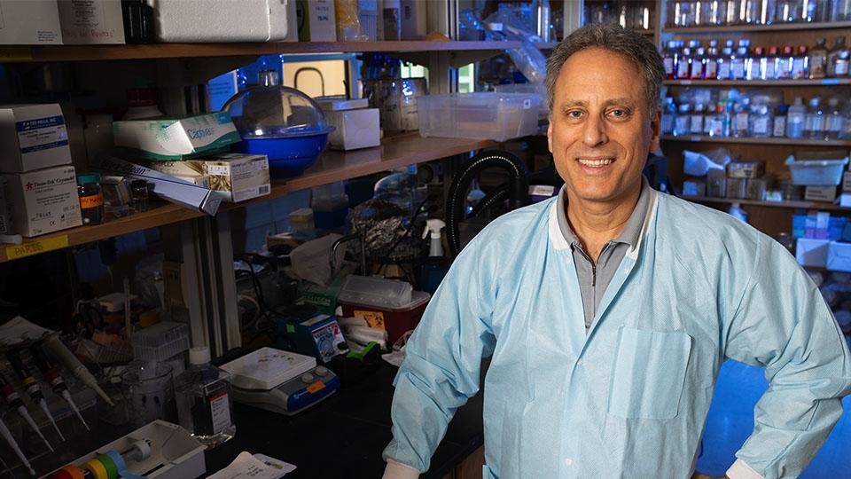
When Mark Prausnitz talks about his work as a professor, researcher, and entrepreneur, one theme comes through clearly: collaboration.
Prausnitz, a Regents’ Professor, Regents’ Entrepreneur, and J. Erskine Love Jr. Chair in the School of Chemical and Biomolecular Engineering, is this year’s recipient of the Class of 1934 Distinguished Professor Award.
“While I may be the focal point, it’s not a recognition of me as an individual. It’s a recognition of everything the team has done,” Prausnitz said. “I know how to do some things, but there are many things I don’t know how to do. That’s why working with others matters. You bring people together, fill in the gaps, and solve the whole problem.”
The “some things” Prausnitz knows how to do have led to revolutionary medical innovation over a 30-year career at Georgia Tech, where he has led transformative work in microneedle drug delivery, launching 10 companies in the process.
During that time, Prausnitz published hundreds of peer-reviewed papers, was granted dozens of patents, and advanced his work from early laboratory studies into more than 20 human clinical trials. His research has produced multiple FDA‑approved or clinically tested technologies.
Understanding Prausnitz’s success starts with his approach to engineering in practice. Science may begin with discovery, but engineering, as he describes it, focuses on taking something uncertain and making it work.
“One of the things that really distinguishes engineering from science is the work of problem-solving to reach an answer,” he said. “You start with something diffuse and figure out how to put all the pieces together. That to me is a hallmark of engineering.”
That way of thinking took shape early in his life.
Julian Hills | Executive Communications Specialist
Institute Communications
Joint Workshop Highlights Emerging Research at the Intersection of Sustainability, Mobility, and Health
Apr 23, 2026 —
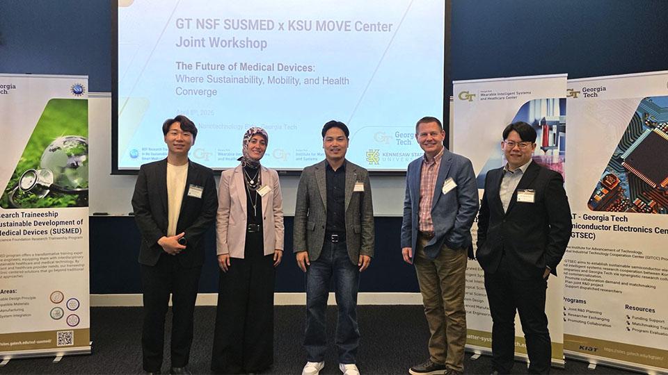
Students, faculty, and researchers from Georgia Tech and Kennesaw State University gathered on April 8 for a joint workshop between Georgia Tech's NSF Sustainable Development of Smart Medical Devices (SUSMED) program and KSU's Mobility for Everyone (MOVE) Center. The full-day event explored how sustainable design, mobility science, and health technologies are converging to shape the next generation of medical devices.
Hosted in Georgia Tech’s Marcus Nanotechnology Building, the workshop brought together trainees from the NSF SUSMED program and students from the MOVE Center for a day of presentations, posters, and hands‑on demonstrations.
The event was co‑led by Hong Yeo, Peterson Professor in Pediatric Research in the George W. Woodruff School of Mechanical Engineering at Georgia Tech; Karam Kim, research faculty at the same school; and Ayse Tekes, associate professor in Mechanical Engineering at KSU.
“I am thrilled to have hosted this first joint event between the NSF NRT in the WISH Center at Georgia Tech and the KSU MOVE Center. When I first envisioned it, I hoped it would spark meaningful conversations between students and researchers — but what unfolded far exceeded every expectation,” Yeo said. “This was not just a gathering; it was a launchpad for exciting new collaborative projects, dynamic student exchange programs, and bold, ambitious bets on the future of our field. A heartfelt thank you to IMS Director Eric Vogel, Josh Lee, the WISH Center program manager, and Karam Kim, research faculty extraordinaire — none of this would have been possible without their support.”
A central goal of the workshop was to give students meaningful opportunities to present their research and engage with peers across disciplines. According to Tekes, who is the director of the MOVE Center, events like this play a critical role in shaping early career researchers.
“I think these events are very eye-opening,” Tekes said. “They give students a real opportunity to showcase their results, but also to collaborate and learn about research outside their own area. Seeing work across disciplines sparks new questions and helps them think differently.”
Throughout the day, students presented projects on wearable devices, mobility technologies, digital health tools, sustainable engineering approaches, and more. Tekes emphasized how valuable it is for students to practice communicating their work to a broad audience.
“They are getting the practice to present their outputs — the key outcomes of their research — and explain the significance and importance,” she said. “They’re also learning to answer questions from different perspectives, because in this room you’re seeing engineers, computer scientists, and clinicians.”
Due to the strong turnout and enthusiastic participation throughout the day, organizers are already planning another session next semester. By bringing together diverse expertise from both schools, the event highlighted the shared commitment to developing medical technologies that improve mobility, health, and quality of life.
Funding sources: NSF NRT-FW-HTF: NSF Traineeship in the Sustainable Development of Smart Medical Devices (Award # 2345860) and WISH Center grant from the Institute for Matter and Systems
Ashlie Bowman | Communications Manager
Parker H. Petit Institute for Bioengineering and Bioscience
Written by Scarlett Smith
Georgia Tech Authors Celebration 2026
Georgia Tech faculty and staff are invited to join the Office of the Executive Vice President for Research and the Library for the annual Georgia Tech Authors Celebration Wednesday, Feb. 18 from 4:30 to 6:15 p.m. in the Scholars Event Theater, located on Price Gilbert's first floor.
The annual Georgia Tech Authors Celebration is an inspiring event that shines a spotlight on the incredible scholarship happening across campus.
A New Metal Design for Solid-State Batteries
Jun 05, 2025 — Atlanta, GA

Sun Geun Yoon works in a glove box in McDowell’s laboratory at Georgia Tech. [Photo by Christopher McKenney]
Lithium-ion batteries power everything from electric cars to laptops to leaf blowers. Despite their widespread adoption, lithium-ion batteries carry limited amounts of energy, and rare overheating can lead to safety concerns. Consequently, for decades, researchers have sought a more reliable battery.
Solid-state batteries are less flammable and can hold more energy, but they often require intense pressure to function. This requirement has made them difficult to use in applications, but new research from Georgia Tech could change that.
The research group of Matthew McDowell, professor and Carter N. Paden Jr. Distinguished Chair in the George W. Woodruff School of Mechanical Engineering and the School of Materials Science and Engineering, has designed a new metal for solid-state batteries that enables operation at lower pressures. While lithium metal is often used in these batteries, McDowell’s group discovered that combining lithium with softer sodium metal results in improved performance and novel behavior.
McDowell and his collaborators presented their findings in the paper, “Interface Morphogenesis with a Deformable Secondary Phase in Solid-State Lithium Batteries,” published in Science on June 5.
Stackable Solution
Lithium-ion batteries have been the industry standard because they combine compact size, reliability, and longevity. However, they contain a liquid “electrolyte,” which helps lithium ions move in the battery but is also flammable. In solid-state batteries, this electrolyte is a solid material that is less flammable. The challenge is that when the battery is used, the lithium metal in the battery changes its shape, potentially losing contact with the solid electrolyte, which degrades performance. A common way to ensure the metal doesn’t lose contact is to apply high pressure to these batteries.
“A solid-state battery usually requires metal plates to apply this high pressure, and those plates can be bigger than the battery itself,” McDowell said. “This makes the battery too heavy and bulky to be effective.”
The researchers, led by Georgia Tech research scientist Sun Geun Yoon, sought a solution. The solid-state batteries would still require some pressure to function, but they found that by also using a softer metal, less pressure is required. The researchers decided to pair the commonly used lithium metal with a surprising element: sodium.
“Adding sodium metal is the breakthrough,” McDowell noted. “It seems counterintuitive because sodium is not active in the battery system, but it’s very soft, which helps improve the performance of the lithium.”
How soft can sodium be? In a controlled environment, a person could stick their gloved finger into sodium metal and leave an imprint.
From Biology to Battery
To understand the enhanced performance of their battery, the researchers borrowed a concept from biology called morphogenesis. This concept explains how tissues or other biological structures evolve based on local stimuli. Morphogenesis is rarely seen in materials science, but the researchers found that the combination of lithium and sodium behaves according to this concept.
McDowell’s research group has been working on applying morphogenesis to battery materials as part of a project funded by the Defense Advanced Research Projects Agency in collaboration with several other universities. Their battery is among the first viable demonstrations of this concept — effectively, the sodium deforms readily at the low pressures needed for solid-state batteries to function.
Battery Boon
The possibilities of a viable, smaller solid-state battery are vast. Imagine a phone battery that could last much longer or an electric vehicle that could drive 500 miles between charges. With this in mind, McDowell and his team have filed for a patent for this battery system.
While solid-state batteries still have some way to go before commercial use, results like these could mean that solid-state batteries can compete with lithium-ion. McDowell’s lab continues to experiment with other materials to further improve performance.
Funding from the Defense Advanced Research Projects Agency.
Tess Malone, Senior Research Writer/Editor
tess.malone@gatech.edu
Georgia Tech Authors Celebration 2025
2024 Science and Engineering Day at Georgia Tech | Atlanta Science Festival Kickoff - Cloned
Members of the Georgia Tech community are opening their doors once again as part of the 11th annual Atlanta Science Festival. This year, Science and Engineering Day at Georgia Tech will serve as the kickoff event for the entire festival!
(Re)Working AI: Designing workplace technologies with and for labor
Speaker: Sarah Fox, Assistant Professor at Carnegie Mellon University in the Human Computer Interaction Institute
Read & Publish Reception
Join us Wednesday, Oct. 16 from 4:30 to 6 p.m. in the Scholars Event Theater, located on Price Gilbert's first floor, to celebrate a transformative step towards Open Access at the Georgia Tech Library's first ever Read & Publish Reception.
Georgia Tech EVPR Chaouki Abdallah Named President of Lebanese American University
Jun 25, 2024 — Atlanta

Chaouki Abdallah, Georgia Tech's executive vice president for Research (EVPR), has been named the new president of the Lebanese American University in Beirut.
Abdallah, MSECE 1982, Ph.D. ECE 1988, has served as EVPR since 2018; in this role, he led extraordinary growth in Georgia Tech's research enterprise. Through the work of the Georgia Tech Research Institute, 10 interdisciplinary research institutes (IRIs), and a broad portfolio of faculty research, Georgia Tech now stands at No. 17 in the nation in research expenditures — and No. 1 among institutions without a medical school.
Additionally, Abdallah has also overseen Tech's economic development activities through the Enterprise Innovation Institute and such groundbreaking entrepreneurship programs as CREATE-X, VentureLab, and the Advanced Technology Development Center.
Under Abdallah's strategic, thoughtful leadership, Georgia Tech strengthened its research partnerships with historically Black colleges and universities, launched the New York Climate Exchange with a focus on accelerating climate change solutions, established an AI Hub to boost research and commercialization in artificial intelligence, advanced biomedical research (including three research awards from ARPA-H), and elevated the Institute's annual impact on Georgia's economy to a record $4.5 billion.
Prior to Georgia Tech, Abdallah served as the 22nd president of the University of New Mexico (UNM), where he also had been provost, executive vice president of academic affairs, and chair of the electrical and computer engineering department. At UNM, he oversaw long-range academic planning, student success initiatives, and improvements in retention and graduation rates.
A national search will be conducted for Abdallah's replacement. In the coming weeks, President Ángel Cabrera will name an interim EVPR.