Georgia Tech Joins Global Industrial Technology Cooperation Center to Advance Semiconductor Electronics Research
May 29, 2024 —
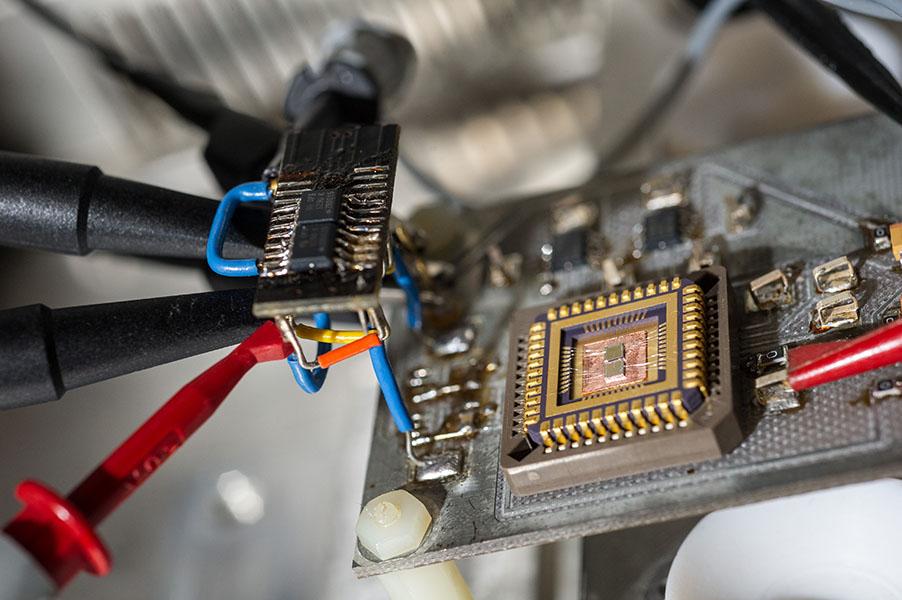
Georgia Tech has been selected as one of six universities globally to receive funding for the newly established Global Industrial Technology Cooperation Center. The announcement was made by the Ministry of Trade, Industry, and Energy in South Korea during the Global Open Innovation Strategy Meeting in April.
The KIAT-Georgia Tech Semiconductor Electronics Center will receive $1.8 million to establish a sustainable semiconductor electronics research partnership between Korean companies, researchers, and Georgia Tech.
“I am thrilled to announce that we have secured funding to launch a groundbreaking collaboration between Georgia Tech’s world-class researchers and Korean companies,” said Hong Yeo, associate professor and Woodruff Faculty Fellow in the George W. Woodruff School of Mechanical Engineering and the Wallace H. Coulter Department of Biomedical Engineering. “This initiative will drive the development of cutting-edge technologies to advance semiconductor, sensors, and electronics research.”
Yeo will lead the center, and Michael Filler, interim executive director for the Institute of Electronics and Nanotechnology, and Muhannad Bakir, director of the 3D Advanced Packaging Research Center, will serve as co-PIs.
The center will focus on advancing semiconductor research, a critical area of technology that forms the backbone of modern electronics.
The Cooperation Center is a global technology collaboration platform designed to facilitate international joint research and development planning, partner matching, and local support for domestic researchers. The selection of Georgia Tech underscores the Institute’s leadership and expertise in the field of semiconductors.
Amelia Neumeister
Research Communications Program Manager
Biden-Harris Administration Announces Preliminary Terms with Absolics to Support Development of Glass Substrate Technology for Semiconductor Advanced Packaging
May 23, 2024 —

The Biden-Harris Administration announced that the U.S. Department of Commerce and Absolics, an affiliate of the Korea-based SKC, have signed a non-binding preliminary memorandum of terms to provide up to $75 million in direct funding under the CHIPS and Science Act to help advance U.S. technology leadership. The proposed investment would support the construction of a 120,000 square-foot facility in Covington, Georgia and the development of substrates technology for use in semiconductor advanced packaging. Started through a collaboration with the 3D Packaging Research Center at Georgia Tech, Absolics’ project serves as an example of American lab-to-fab development and production.
"Glass-core packaging holds the promise to revolutionize the field of advanced packaging and impact major paradigms such as artificial intelligence, mm-wave/THz communication, and photonic connectivity," said Muhannad Bakir, Dan Fielder Professor in the School of Electrical and Computer Engineering and Director of the 3D Systems Packaging Research Center at Georgia Tech. "We look forward to supporting Absolics in establishing a glass-core packaging facility in the State of Georgia through workforce development initiatives."
Because of President Biden’s CHIPS and Science Act, this proposed investment would support over an estimated 1,000 construction jobs and approximately 200 manufacturing and R&D jobs in Covington and enhance innovation capacity at Georgia Institute of Technology, supporting the local semiconductor talent pipeline.
The proposed investment with Absolics is the first proposed CHIPS investment in a commercial facility supporting the semiconductor supply chain by manufacturing a new advanced material.
Amelia Neumeister
Research Communications Program Manager
Family Loss Brings About Medical Breakthrough
May 14, 2024 —

Hong Yeo shows off the latest version of his wearable sleep monitoring device.
The call from his mom is still vivid 20 years later. Moments this big and this devastating can define lives, and for Hong Yeo, today a Georgia Tech mechanical engineer, this call certainly did. Yeo was a 21-year-old in college studying car design when his mom called to tell him his father had died in his sleep. A heart attack claimed the life of the 49-year-old high school English teacher who had no history of heart trouble and no signs of his growing health threat. For the family, it was a crushing blow that altered each of their paths.
“It was an uncertain time for all of us,” said Yeo. “This loss changed my focus.”
For Yeo, thoughts and dreams of designing cars for Hyundai in Korea turned instead toward medicine. The shock of his father going from no signs of illness to gone forever developed into a quest for medical answers that might keep other families from experiencing the pain and loss his family did — or at least making it less likely to happen.
Yeo’s own research and schooling in college pointed out a big problem when it comes to issues with sleep and how our bodies’ systems perform — data. He became determined to invent a way to give medical doctors better information that would allow them to spot a problem like his father’s before it became life-threatening.
His answer: a type of wearable sleep data system. Now very close to being commercially available, Yeo’s device comes after years of working on the materials and electronics for an easy-to-wear, comfortable mask that can gather data about sleep over multiple days or even weeks, allowing doctors to catch sporadic heart problems or other issues. Different from some of the bulky devices with straps and cords currently available for at-home heart monitoring, it offers the bonuses of ease of use and comfort, ensuring little to no alteration to users’ bedtime routine or wear. This means researchers can collect data from sleep patterns that are as close to normal sleep as possible.
“Most of the time now, gathering sleep data means the patient must come to a lab or hospital for sleep monitoring. Of course, it’s less comfortable than home, and the devices patients must wear make it even less so. Also, the process is expensive, so it’s rare to get multiple nights of data,” says Audrey Duarte, University of Texas human memory researcher.
Duarte has been working with Yeo on this system for more than 10 years. She says there are so many mental and physical health outcomes tied to sleep that good, long-term data has the potential to have tremendous impact.
“The results we’ve seen are incredibly encouraging, related to many things —from heart issues to areas I study more closely like memory and Alzheimer’s,” said Duarte.
Yeo’s device may not have caught the arrhythmia that caused his father’s heart attack, but nights or weeks of data would have made effective medical intervention much more likely.
Inspired by his own family’s loss, Yeo’s life’s work has become a tool of hope for others.
Blair.Meeks@gatech.edu
Institute for Electronics and Nanotechnology Builds the Future Microelectronics Workforce
May 02, 2024 —

When Amy Bonecutter-Leonard was a second-semester undergraduate at the Georgia Institute of Technology, she applied for a work-study job in the cleanroom at the Microelectronics Research Center (MiRC). There, she learned process techniques for making the same type of electronic chips used in cellphones.
With this new knowledge, she could train and help other students with their research. At the time, Bonecutter-Leonard was a chemical engineering major with no plans to go into microelectronics. Working in the cleanroom changed that.
“I fell in love with microelectronics through exposure to the research and development work performed in the cleanroom,” she said.
What started as a student job led to her taking microelectronics classes — and eventually to a career in the field. “My work-study prepared me with hands-on technical skills I would have never learned from just being in a classroom,” she said. Now, Bonecutter-Leonard works as a microelectronics business chief engineer at defense contractor L3Harris Technologies.
Her story is one of many from the Institute for Electronics and Nanotechnology (IEN, the successor to MiRC), which has been training students from kindergarten to graduate school to be leaders in the microelectronics and nanotechnology space. The goal of IEN’s outreach is to make nanotechnology and microelectronics — such as computer chips and sensors — as accessible as any other science. Ultimately, these efforts will build up the U.S. workforce in the field, ensuring the country remains at the forefront of the technology that powers Americans’ everyday lives.
Building the Workforce
Bolstering the number of workers in the microelectronics industry is imperative to keep the U.S. globally competitive. Right now, 40% of the industry's labor force is older than 50, with practitioners aging out of their careers at a pace new talent cannot match. Additionally, heavy educational barriers to entry, including required degrees and specialized training, prevent more people from pursuing careers in the field. Without dedicated efforts, the entire sector — and the nation — will fall behind.
IEN is working to solve this pipeline problem.
“With the national semiconductor workforce aging, it is important now more than ever that we educate the next generation to move into these jobs,” said Michael Filler, IEN’s interim executive director. “IEN is proud to support the semiconductor industry by providing students with the interdisciplinary skills and hands-on technical training essential for success in this fast-paced, global field.”
Georgia Tech is uniquely positioned to lead this charge with its 28,500 square feet of academic cleanroom space, the largest in the Southeast and among the largest in the U.S. From micro-electro-mechanical systems to electronics fabrication, workers have 100 bays in which to conduct leading-edge research. These cleanrooms are also key teaching and training facilities.
IEN invites anyone from around the world, whether affiliated with the Institute or not, to become a core user of the cleanroom facilities. The center also regularly hosts short courses for external partners — academic, industry, and government — in microfabrication and soft lithography for microfluidics. Over the past three years, more than 700 people went through new-user orientation, and 193 enrolled in the short courses.
Teaching the Next Generation
Making nanotechnology — of which microelectronics is an example — educationally accessible begins before college. Each semester, more than 800 K-12 students participate in IEN’s Introduction to Nanotechnology virtual lesson. Associate Director for Education and Outreach Mikkel Thomas begins his presentations by asking a simple question: What do you know about nanotechnology?
“About 99% of the time, they say that’s what makes Ironman’s suit work,” said Thomas. “That means they’ve learned the wrong lesson — that nanotechnology is a futuristic tech and that you have to be as smart as Tony Stark to work in the field.
“But most people interact with nanotechnology multiple times throughout their day, and they have no idea they're doing it.”
Thomas also emphasizes there is a career path for everyone, even if they don’t plan to get a traditional four-year degree. Part of IEN’s workforce development initiative is to build up the entire pipeline from industry and research lab technicians at the certificate level to postdoctoral researchers.
“It’s important for us to reach kids who don’t know what career options are available in nanotechnology,” Thomas said. “We want them to know that whatever they're interested in, there is a pathway for them.”
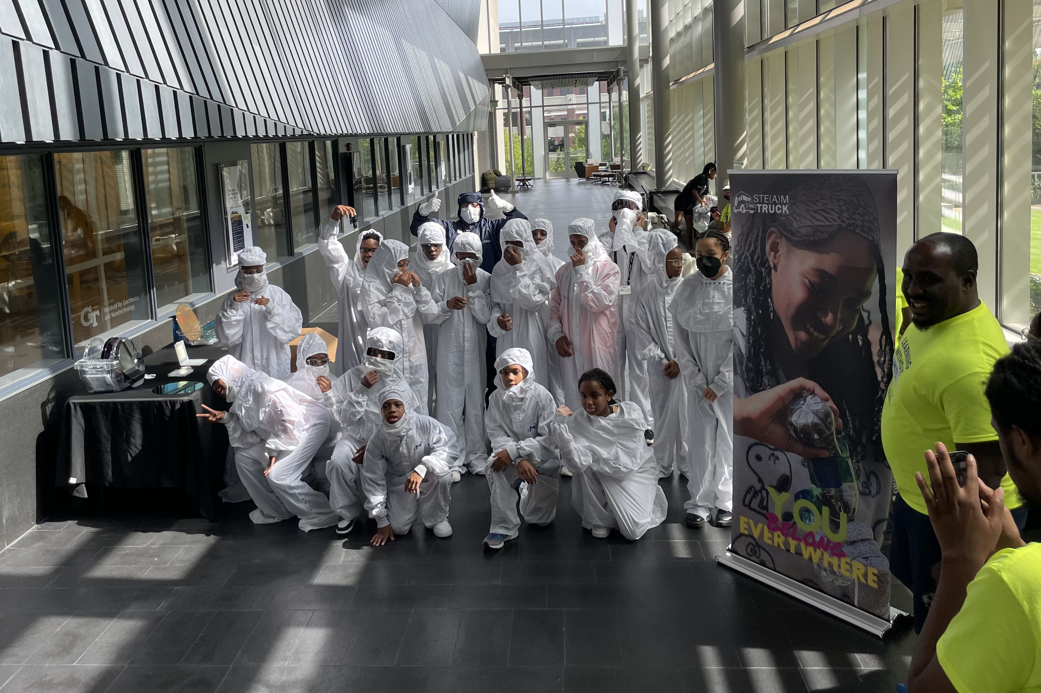
Sixth- through eighth-grade students sparked by this conversation can attend Chip Camp, a three-day STEM summer camp sponsored by Micron. They begin with a day at IEN to learn about thin films, magic sands, ferrofluids, and measuring their height in nanometers. The rest of the camp features hands-on visits to the Materials Characterization Facility (MCF) and the IEN cleanroom, where they can try on the white “bunny suits” technicians wear in the lab.
To further their reach, IEN’s workforce development team collaborates with teachers to bring nanotechnology into classrooms. During the summer, IEN offers the Research Experience for Teachers, a training program for public school and community college teachers to conduct nanotechnology research and learn how to incorporate it into their lessons. Middle school teachers have similar opportunities through the Nanoscience Summer Institute for Middle School Teachers.
Training the Workforce
When these students get to a university like Georgia Tech, IEN hires them for work-study jobs like the one Bonecutter-Leonard had. The hands-on cleanroom training is also vital to graduate students pursuing advanced degrees.
Katie Young earned her Ph.D. in materials science and engineering at Georgia Tech. Learning her way around the IEN cleanroom was essential for her graduate studies.
“My dissertation research involved synthesizing two-dimensional materials — only a single atom thick — for permeation barriers,” she explained. “I often used the cleanroom’s vacuum systems to synthesize and process 2D materials.” Now a research scientist at the Georgia Tech Research Institute, Young still works in the cleanroom on semiconductor device fabrication, building prototype quantum and biological sensors.
IEN opportunities are not limited to graduate research. Annually, about 150 Georgia Tech undergraduate students take microelectronics packaging and devices classes, with labs taught by IEN staff in the teaching cleanroom. These courses include Integrated Circuit Fabrication (ECE 4452), in which students learn to fabricate circuit elements, and the Science and Engineering of Microelectronic Fabrication (ChBE 4050/6050, open to graduate students as well), for students interested in semiconductor materials and fabrication.
Students don’t need to enroll at Georgia Tech to benefit from training, courses, and other opportunities. IEN’s internship program provides technical college students with training to become microelectronics technicians, either through work in the Biocleanroom or in the MCF.
Empowering Future Innovators
IEN also participates in the National Science Foundation Research Experiences for Undergraduates (REU), which provides opportunities for students from underrepresented groups or who attend schools without similar facilities. While enrolled at another university, John Mark Page was introduced to Georgia Tech’s cleanroom through an REU.
“That was my first exposure to any facility of this kind, and it felt like I was looking at the future. Being in a facility that can fabricate devices at or near the atomic level — it was hard to fathom,” Page said. “I had never thought that participating in microelectronics and nanotechnology as a student, especially as an undergraduate, was something I could do.”
As a result of his REU, Page transferred to Georgia Tech — he will graduate this summer with a bachelor’s degree in electrical engineering. He also completed a second REU at the University of North Carolina at Chapel Hill, worked as a student assistant in the IEN cleanroom, and participated in a Vertically Integrated Project (VIP), Chip Scale Power and Energy.
“I was interested in the VIP because it allowed me to spend more time in the cleanroom, familiarizing myself with semiconductor fabrication methods and training on new fabrication equipment,” Page explained. His experiences inspired him to consider a future career in the semiconductor industry.
“It wasn’t only the 10-week experience of the REU that made a lasting impact on me,” he said. “It was also the relationships formed with the people of IEN. The staff there are exceptional representatives of Georgia Tech, and they make IEN a tremendous asset to the future of microelectronics and nanotechnology in the U.S.”
Biya Haile, an ECE Ph.D. student, had a similarly meaningful REU experience. Haile, whose research focuses on creating micro-electro-mechanical systems-based sensors (MEMS), described the REU as “immersive.”
“The REU project enabled me to study chemical micro-sensor technologies, as well as state-of-the-art additive nano-manufacturing techniques, which has contributed to my research,” he said. “I feel lucky that my academic journey has entailed developing new technologies that use nanoscience to solve big problems.”
While Haile is currently focused more on designing and testing rapid processes for fabricating MEMS-based devices, he still occasionally works in the cleanroom on fabrication. He plans to go into the microelectronics industry after graduating.
The Path Ahead
All of IEN’s training and educational offerings align with IEN’s mission to bolster and diversify the microelectronics workforce, according to George White, senior director of strategic partnerships for the Georgia Tech research enterprise. “IEN has been at the forefront of the CHIPS infrastructure buildout, particularly in the area of education and workforce development,” he noted.
IEN’s efforts impact not just Atlanta but the entire country. Georgia Tech’s leadership in microelectronics research trains the innovators and practitioners of the future everywhere and ensures that America stays at the forefront of leading-edge technology. As demand increases for microelectronics, IEN is moving to meet it.
Effective July 1, 2024, the Institute for Electronics and Nanotechnology and the Institute for Materials will evolve into the Institute for Matter and Systems (IMS). This strategic union aims to foster convergent research at Georgia Tech, focusing on the science, technology, and societal underpinnings of cutting-edge materials and devices. Eric Vogel will be the director of IMS, and Michael Filler will be the deputy director.
Media Contact: Tess Malone, Senior Research Writer/Editor tess.malone@gatech.edu
Physicists Pioneer New Quantum Sensing Platform
May 02, 2024 —

Quantum sensors detect the smallest of environmental changes — for example, an atom reacting to a magnetic field. As these sensors “read” the unique behaviors of subatomic particles, they also dramatically improve scientists’ ability to measure and detect changes in our wider environment.
Monitoring these tiny changes results in a wide range of applications — from improving navigation and natural disaster forecasting, to smarter medical imaging and detection of biomarkers of disease, gravitational wave detection, and even better quantum communication for secure data sharing.
Georgia Tech physicists are pioneering new quantum sensing platforms to aid in these efforts. The research team’s latest study, “Sensing Spin Wave Excitations by Spin Defects in Few-Layer Thick Hexagonal Boron Nitride” was published in Science Advances this week.
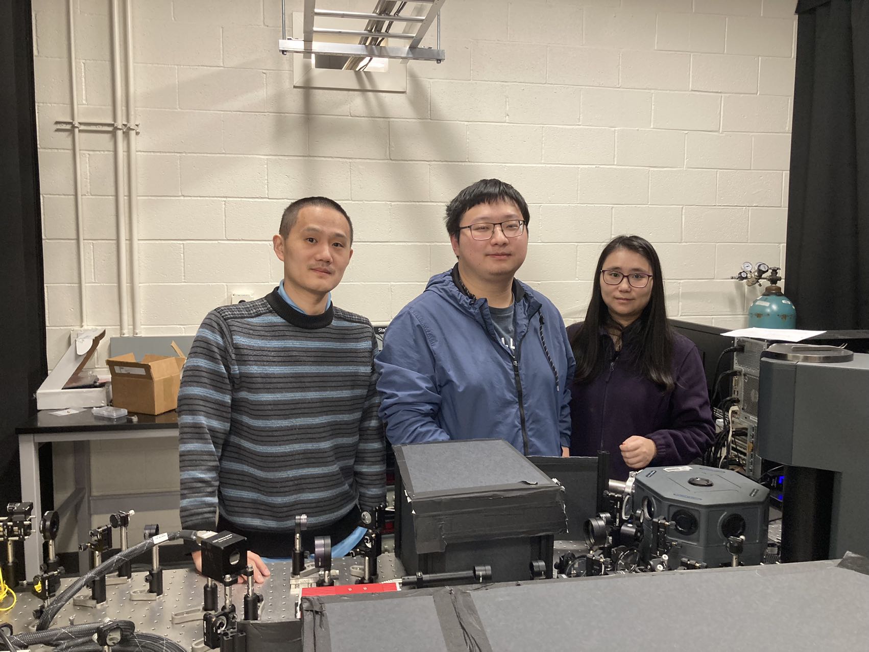
The research team includes School of Physics Assistant Professors Chunhui (Rita) Du and Hailong Wang (corresponding authors) alongside fellow Georgia Tech researchers Jingcheng Zhou, Mengqi Huang, Faris Al-matouq, Jiu Chang, Dziga Djugba, and Professor Zhigang Jiang and their collaborators.
An ultra-sensitive platform
The new research investigates quantum sensing by leveraging color centers — small defects within crystals (Du’s team uses diamonds and other 2D layered materials) that allow light to be absorbed and emitted, which also give the crystal unique electronic properties.
By embedding these color centers into a material called hexagonal boron nitride (hBN), the team hoped to create an extremely sensitive quantum sensor — a new resource for developing next-generation, transformative sensing devices.
For its part, hBN is particularly attractive for quantum sensing and computing because it could contain defects that can be manipulated with light — also known as "optically active spin qubits."
The quantum spin defects in hBN are also very magnetically sensitive, and allow scientists to “see” or “sense” in more detail than other conventional techniques. In addition, the sheet-like structure of hBN is compatible with ultra-sensitive tools like nanodevices, making it a particularly intriguing resource for investigation.
The team’s research has resulted in a critical breakthrough in sensing spin waves, Du says, explaining that “in this study, we were able to detect spin excitations that were simply unattainable in previous studies.”
Detecting spin waves is a fundamental component of quantum sensing, because these phenomena can travel for long distances, making them an ideal candidate for energy-efficient information control, communication, and processing.
The future of quantum
“For the first time, we experimentally demonstrated two-dimensional van der Waals quantum sensing — using few-layer thick hBN in a real-world environment,” Du explains, underscoring the potential the material holds for precise quantum sensing. “Further research could make it possible to sense electromagnetic features at the atomic scale using color centers in thin layers of hBN.”
Du also emphasizes the collaborative nature of the research, highlighting the diverse skill sets and resources of researchers within Georgia Tech.
“Within the School of Physics, Professor Zhigang Jiang's research group provided the team with high-quality hBN crystals. Jingcheng Zhou, who is a member of both Professor Hailong Wang’s and my research teams, performed the cutting-edge quantum sensing measurements,” she says. “Many incredible students also helped with this project.”
Du is a leading scientist in the field of quantum sensing — this year, she received a new grant from the U.S. Department of Energy, along with a Sloan Research Fellowship for her pioneering work on developing state-of-the-art quantum sensing techniques for quantum information technology applications. The prestigious Sloan award recognizes researchers whose “creativity, innovation, and research accomplishments make them stand out as the next-generation of leaders in the fields.”
This work is supported by the U. S. National Science Foundation (NSF) under award No. DMR-2342569, the Air Force Office of Scientific Research under award No. FA9550-20-1-0319 and its Young Investigator Program under award No. FA9550-21-1-0125, the Office of Naval Research (ONR) under grant No. N00014-23-1-2146, NASA-REVEALS SSERVI (CAN No. NNA17BF68A), and NASA-CLEVER SSERVI (CAN No. 80NSSC23M0229).
Written by Selena Langner
Contact: Jess Hunt-Raston
Director of Communications
College of Sciences at Georgia Tech
Georgia Tech and Meta Create Massive Open Dataset to Advance AI Solutions for Carbon Capture
May 02, 2024 — Atlanta

A Georgia Tech researcher examines a component of a direct air capture system that employs carbon fiber strands. Direct air capture systems require chemical materials that can grab carbon dioxide.
To avoid catastrophic climate impacts, excessive carbon emissions must be addressed. At this point, cutting emissions isn’t enough. Direct air capture, a technology that pulls carbon dioxide out of ambient air, has great potential to help solve the problem.
But there’s a big challenge. For direct air capture technology, every type of environment and location requires a uniquely specific design. A direct air capture configuration in Texas, for example, would necessarily be different from one in Iceland. These systems must be designed with exact parameters for humidity, temperature, and air flows for each place.
Now, Georgia Tech and Meta have collaborated to produce a massive database, potentially making it easier and faster to design and implement direct air capture technologies. The open-source database enabled the team to train an AI model that is orders of magnitude faster than existing chemistry simulations. The project, named OpenDAC, could accelerate climate solutions the planet desperately needs.
The team’s research was published in ACS Central Science, a journal of the American Chemical Society.
“For direct air capture, there are many ideas about how best to take advantage of the air flows and temperature swings of a given environment,” said Andrew J. Medford, associate professor in the School of Chemical and Biomolecular Engineering (ChBE) and a lead author of the paper. “But a major problem is finding a material that can capture carbon efficiently under each environment’s specific conditions.”
Their idea was to “create a database and a set of tools to help engineers broadly, who need to find the right material that can work,” Medford said. “We wanted to use computing to take them from not knowing where to start to giving them a robust list of materials to synthesize and try.”
Containing reaction data for 8,400 different materials and powered by nearly 40 million quantum mechanics calculations, the team believes it’s the largest and most robust dataset of its kind.
Building a Partnership (and a Database)
Researchers with Meta’s Fundamental AI Research (FAIR) team were looking for ways to harness their machine learning prowess to address climate change. They landed on direct air capture as a promising technology and needed to find a partner with expertise in materials chemistry as it relates to carbon capture. They went straight to Georgia Tech.
David Sholl, ChBE professor, Cecile L. and David I.J. Wang Faculty Fellow, and director of Oak Ridge National Laboratory’s Transformational Decarbonization Initiative, is one of the world’s top experts in metal-organic frameworks (MOFs). These are a class of materials promising for direct air capture because of their cagelike structure and proven ability to attract and trap carbon dioxide. Sholl brought Medford, who specializes in applying machine learning models to atomistic and quantum mechanical simulations as they relate to chemistry, into the project.
Sholl, Medford, and their students provided all the inputs for the database. Because the database predicts the MOF interactions and the energy output of those interactions, considerable information was required.
They needed to know the structure of nearly every known MOF — both the MOF structure by itself and the structure of the MOF interacting with carbon dioxide and water molecules.
“To predict what a material might do, you need to know where every single atom is and what its chemical element is,” Medford said. “Figuring out the inputs for the database was half of the problem, and that’s where our Georgia Tech team brought the core expertise.”
The team took advantage of large collections of MOF structures that Sholl and his collaborators had previously developed. They also created a large collection of structures that included imperfections found in practical materials.
The Power of Machine Learning
Anuroop Sriram, research engineering lead at FAIR and first author on the paper, generated the database by running quantum chemistry computations on the inputs provided by the Georgia Tech team. These calculations used about 400 million CPU hours, which is hundreds of times more computing than the average academic computing lab can do in a year.
FAIR also trained machine learning models on the database. Once trained on the 40 million calculations, the machine learning models were able to accurately predict how the thousands of MOFs would interact with carbon dioxide.
The team demonstrated that their AI models are powerful new tools for material discovery, offering comparable accuracy to traditional quantum chemistry calculations while being much faster. These features will allow other researchers to extend the work to explore many other MOFs in the future.
“Our goal was to look at the set of all known MOFs and find those that most strongly attract carbon dioxide while not attracting other air components like water vapor, and using these highly accurate quantum computations to do so,” Sriram said. “To our knowledge, this is something no other carbon capture database has been able to do.”
Putting their own database to use, the Georgia Tech and Meta teams identified about 241 MOFs of exceptionally high potential for direct air capture.
Moving Forward With Impact
“According to the UN and most industrialized countries, we need to get to net-zero carbon dioxide emissions by 2050,” said Matt Uyttendaele, director of Meta’s FAIR chemistry team and a co-author on the paper. “Most of that must happen by outright stopping carbon emissions, but we must also address historical carbon emissions and sectors of the economy that are very hard to decarbonize — such as aviation and heavy industry. That’s why CO2 removal technologies like direct air capture must come online in the next 25 years.”
While direct air capture is still a nascent field, the researchers say it’s crucial that groundbreaking tools — like the OpenDAC database made available in the team’s paper — are in development now.
“There is not going to be one solution that will get us to net-zero emissions,” Sriram said. “Direct air capture has great potential but needs to be scaled up significantly before we can make a real impact. I think the only way we can get there is by finding better materials.”
The researchers from both teams hope the scientific community will join the search for suitable materials. The entire OpenDAC dataset project is open source, from the data to the models to the algorithms.
“I hope this accelerates the development of negative-emission technologies like direct air capture that may not have been possible otherwise,” Medford said. “As a species, we must solve this problem at some point. I hope this work can contribute to getting us there, and I think it has a real shot at doing that.”
Note: Georgia Tech ChBE graduate students Sihoon Choi, Logan Brabson, and Xiaohan Yu made major contributions and are co-authors of the paper.
Citation: A. Sriram et al, The Open DAC 2023 Dataset and Challenges for Sorbent Discovery in Direct Air Capture, ACS Central Science (2024).
DOI: https://doi.org/10.1021/acscentsci.3c01629
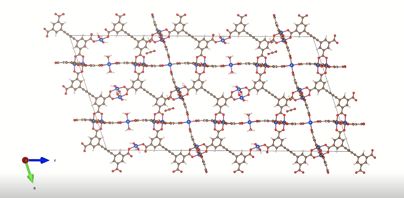
A visualization of a metal-organic framework. (Credit: Logan Brabson)
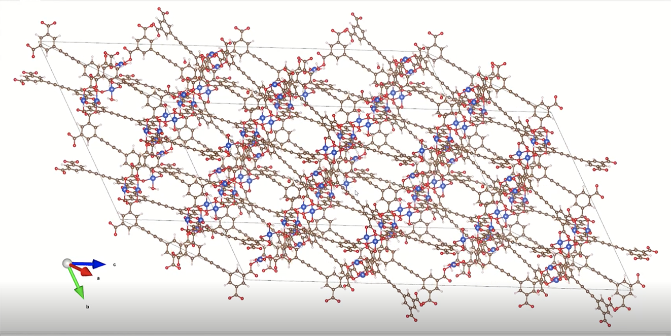
A visualization of the same metal-organic framework, which has been rotated to show porosity and dimension. (Credit: Logan Brabson)
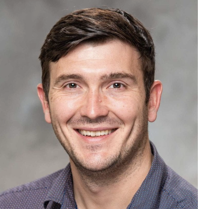
Andrew J. Medford, associate professor in the School of Chemical and Biomolecular Engineering (ChBE).
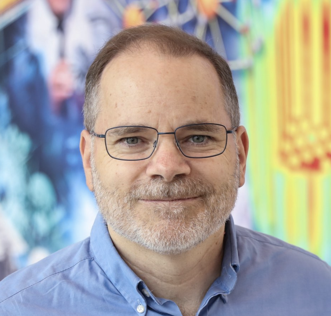
David Sholl, ChBE professor, Cecile L. and David I.J. Wang Faculty Fellow, and director of Oak Ridge National Laboratory’s Transformational Decarbonization Initiative
Catherine Barzler, Senior Research Writer/Editor
New Approach Could Make Reusing Captured Carbon Far Cheaper, Less Energy-Intensive
Apr 25, 2024 — Atlanta, GA

A new electrochemical reactor design developed with Marta Hatzell by postdoctoral scholar Hakhyeon Song (middle) and Ph.D. students Carlos Fernández and Po-Wei Huang (seated) converts carbon dioxide removed from the air into useful raw material. Their approach is cheaper and simpler while requiring less energy, making it a promising tool to improve the economics of direct air capture systems. (Photo: Candler Hobbs)
Engineers at Georgia Tech have designed a process that converts carbon dioxide removed from the air into useful raw material that could be used for new plastics, chemicals, or fuels.
Their approach dramatically reduces the cost and energy required for these direct air capture (DAC) systems, helping improve the economics of a process the researchers said will be critical to addressing climate change.
The key is a new kind of catalyst and electrochemical reactor design that can be easily integrated into existing DAC systems to produce useful carbon monoxide (CO) gas. It’s one of the most efficient such design ever described in scientific literature, according to lead researcher Marta Hatzell and her team. They published details April 16 in Energy and Environmental Science, a top journal for energy-related research.
Joshua Stewart
College of Engineering
Machine-Vision In-Situ TEM, Worfkow Solutions, Data Management and AI Platform Seminar
AGENDA
10:00 AM - 10:10 AM
Welcome and Introduction
Gabriela Mendoza, US Central Sales Manager
10:10 AM - 10:50 AM
Presentation: In-Situ TEM Workflow Solutions
Gabriela Mendoza, US Central Sales Manager
11:00 AM– 11:40 AM
AXON Studio Workshop
Tim Eldred, Product Marketing Manager
SPEAKER
Tim Eldred, Ph.D.
XPS Workshop
Register now to attend this FREE XPS Workshop on May 8th & 9th, 2024 to learn how X-ray Photoelectron Spectroscopy (XPS) can be used to investigate cutting-edge materials via surface chemistry and the elemental as well as electronic state of atoms.
Why you should attend:
- Expand your understanding of XPS for materials analysis.
- Speak directly with experts about today’s instrumentation & how it can work for you.
- Experience hands-on demonstrations and presentations.
