Fall 2022 Short Course on Soft Lithography for Microfluidics
This course module is designed for individuals interested in hands-on training in the fabrication of microfluidic devices using the soft lithography technique. It is structured to assume no prior knowledge of the technologies by the participants. The course agenda is evenly divided between hands-on laboratory sessions, including SU-8 master mold creation using photolithography and PDMS device fabrication in the IEN cleanroom, and supporting lectures.
Georgia Tech’s $26 Million Partnership with National Science Foundation to Transform Fertilizer Production
Aug 10, 2022 — Atlanta, GA

Paul Kohl (School of Chemical and Biomolecular Engineering) and Marta Hatzell (George W. Woodruff School of Mechanical Engineering) will lead CASFER’s efforts at Georgia Tech.
The Center for Advancing Sustainable and Distributed Fertilizer Production (CASFER) is a collaborative effort between the National Science Foundation (NSF) and five universities.
Thanks to efforts to combat climate change, many have heard the catchphrase “closing the carbon loop” — a global effort to convert carbon dioxide into something useful to mitigate the damaging effects of pollution on the planet. Another environmental challenge relates not to carbon dioxide but nitrogen. Now, an ambitious plan to close the nitrogen loop is underway, and with it comes the potential to revolutionize agriculture in the U.S. and around the world.
The Georgia Institute of Technology will be part of CASFER, an NSF Engineering Research Center (NSF-ERC), with four other universities. Supported by an initial grant of $26 million from NSF, CASFER seeks to transform the U.S. from nitrogen cycle pollution to a nitrogen circular economy by developing new technologies and programs for capturing, recycling, and producing decarbonized nitrogen-based fertilizers (NBFs). Georgia Tech is joined by Florida Agricultural and Mechanical University, Case Western Reserve University, the Massachusetts Institute of Technology, and Texas Tech University, which will lead the effort and serve as CASFER’s headquarters.
Nitrogen is used in many commercial applications, but one of the most significant uses is in NBFs for growing food. NBFs are put out into fields, but most do not get used — 80% are washed away and wasted, ending up as pollutants in the watershed. With support from NSF, this team of universities will attempt to recover and reuse nitrogen compounds, the principal element in fertilizers.
“By taking pollutants out of the water and converting them for use, we are taking a negative and making a positive out of it,” said Paul Kohl, Regents' Professor and Thomas L. Gossage Chair in the School of Chemical and Biomolecular Engineering (ChBE) and co-lead of the CASFER effort at Georgia Tech, along with Marta Hatzell, associate professor in the George W. Woodruff School of Mechanical Engineering. “This process will both decrease pollution and lower the cost of farming.”
CASFER has three areas of focus it will pursue to achieve its goal. The first involves measuring and analyzing data to identify new opportunities and locations for collecting wasted fertilizer and determining how exactly the fertilizer affects individual environments.
The second area — Kohl and Hatzell’s focus — is the actual collection and separation of nitrogen compounds from the three types of environments where they usually show up: produce farms, livestock farms, and wastewater treatment plants. They will develop specialized separation methods to pull nitrogen pollutants out of the various environments, creating new types of polymer membranes that work to separate and concentrate the compounds into solutions that can be converted for future use. The work will start in the laboratories at Georgia Tech, but later the team will build test beds — portable laboratories the size of small trailers — to test their separation methods on-site.
“All our separations technologies will be modular, electrified, and largely decarbonized,” said Hatzell. “Our overall goal is to design processes that synthesize new or recover used fertilizers from waste at the same or lower price than traditional chemical manufacturing processes.”
The third area is reconverting the concentrated solutions into usable fertilizer. Humans have been making fertilizer the same way for more than 100 years, using an expensive chemical process that requires natural gas — a resource in short supply. CASFER researchers will develop the conversion methods to create new fertilizers and strategies for dispensing it back into fields for growing crops.
“One strength of NSF Engineering Research Centers is their ability to bring interdisciplinary academic teams together in convergent research to identify novel approaches to thorny societal challenges,” said NSF Assistant Director for Engineering Susan Margulies. “With their unique testbeds and industry partners, the centers innovate and translate solutions that are effective and sustainable.”
CASFER is poised to bring about dramatic changes to the agriculture industry. Since the inception of the Engineering Research Centers program in 1985, the NSF has awarded fewer than 100 grants to open ERCs, which are designed to foster innovation and collaboration between industry leaders, government agencies, and institutions of higher education.
“For decades, NSF Engineering Research Centers have transformed technologies and fostered innovations in the United States through bold research, collaborative partnerships, and a deep commitment to inclusion and broadening participation,” said NSF Director Sethuraman Panchanathan. “The new NSF centers will continue the legacy of impacts that improve lives across the nation.”
Looking to the future, universities will launch workforce development efforts like training and education to prepare a new generation of farmers and scientists for work in the nitrogen circular economy.
Georgia Tech researchers involved in the grant include Kohl (Co-Thrust Leader), Andrew Medford, and Joseph Scott from ChBE; Peter Hesketh (Co-Thrust Leader) and Hatzell (Thrust Leader/Co-PI) from the Woodruff School; Mary-Lynn Realff from the School of Materials Science and Engineering; Lizanne DeStefano (EWD Lead) from CEISMC; and Jie Xu and Milad Navaei from the Georgia Tech Research Institute.
Catherine Barzler, Senior Research Writer/Editor
catherine.barzler@gatech.edu
Georgia Tech’s New Aluminum Nitride-based Semiconductor is Poised to Transform the Industry
Aug 04, 2022 — Atlanta, GA

ECE professor Alan Doolittle’s AlN-based semiconductor findings represent an emerging new area of interdisciplinary research covering materials, physics, and devices.
Alan Doolittle is doing what was once thought impossible: turning an electrical insulator into an ultra-wide bandgap semiconductor. The results have groundbreaking potential for high-power electronics, optoelectronics, and more.
For the past 80 or so years, aluminum nitride (AlN) has been thought of as nothing but an electrical insulator. Because of its high electrical insulating and thermal conductivity properties, it is used frequently in electronic applications to dissipate heat quickly and maintain efficiency.
Researchers at the Georgia Institute of Technology, led by professor Alan Doolittle, are discovering that there is a lot more to AlN than meets the eye, and their promising research shows the material has the potential to transform the semiconductor industry. By leveraging the advantages of AlN, ultra-wide bandgap (UWBG) semiconductors can be used at high-power and high-temperature levels never seen before.
“It’s rare to see such encouraging early results,” said Doolittle, the Joseph M. Pettit Professor in the School for Electrical and Computer Engineering (ECE). “To put things into perspective, AlN has the ability to handle over five times the voltage of other existing wide bandgap semiconductors. It really is the birth of a new semiconductor field.”
For electrical devices, there are two types of semiconducting materials needed: one that carries positive charges (p-type) and one that carries negative charges (n-type). The Doolittle group was able to improve current conduction in p-type AlN by 30,000,000 times and n-type AlN by 6,000 times than prior best results.
The findings, recently published in Advanced Materials and the Journal of Applied Physics, received the Most Valuable Contribution Award at the 2022 Workshop on Compound Semiconductor Materials & Devices, a premier workshop in the U.S. on high performance electronic materials.
Ultra-wide Bandgaps Equal Ultra-wide Applications
Georgia Tech’s AlN-based semiconductor findings represent an emerging new area of interdisciplinary research covering materials, physics, and devices with promising applications for future generations of high-power electronics and optoelectronics, as well as quantum electronics and harsh-environment applications.
Semiconductors can both conduct and insulate electricity, meaning they are necessary for all electronic appliances to operate. Scientists make semiconductor materials by using pure elements (most frequently silicon) and adding intentional impurities to make crystals with the desired electrical, thermal, and optical prosperities.
The bandgap is one of the most important properties of a semiconductor, as it represents the minimum energy required for electrical conduction. It is also the largest factor in determining the voltage at which a device fails (called breakdown), as well as represents the energy/wavelength of light emanating from the semiconductor. UWBG semiconductors can operate at high temperatures, frequencies, and voltages, meaning less semiconductor devices are needed in high voltage circuits which increases performance and efficiency, while reducing costs. Doolittle’s AlN-based semiconductor has the highest bandgap ever demonstrated to have both p and n-type conduction needed for electronics.
“The new AlN-based semiconductor appears to have the ability to withstand voltages at incredibly high levels,” said Doolittle. “Levels that can even withstand some sections of the national utility grid, something no other semiconductor can do.”
With the ability to withstand high voltage and high frequency, AlN-based semiconductors can be utilized in power electronic devices found in automotive, industrial, and consumer applications. The technology could also allow utility grids to more effectively control how much power to transmit and where, a growing demand as old systems integrate with other smart grid innovations and renewable energy sources.
The team used a much lower temperature to grow the AlN crystals than what is normally utilized to create semiconductor materials. The low heat process allows for more precise control of the material’s surface chemistry during creation and is potentially a groundbreaking innovation in its own right.
“That kind of out of the box solution caught a lot of people off guard,” said Doolittle. “It was thought that you couldn’t grow good quality material at this low of temperature, but we’ve shown that it’s possible and has broad applicability.”
AlN’s Impressive Optical Properties
Unlike an incandescent light bulb where a filament is heated to glow and produce light, light-emitting diodes (LEDs) emit light when an electric current flows through a layered semiconductor device. The wide bandgap semiconductor material gallium nitride (GaN) was used to create the first LED blue light in the early 1990s by Isamu Akasaki, Hiroshi Amano, and Shuji Nakamura (for which they won the 2014 Nobel Prize in Physics). Creating the high energy blue LED challenged scientist for decades, as it was the final piece needed to create white light and full-color LED displays that have now revolutionized lighting technology and is predicted to save nearly 20% in energy consumption in the U.S. when fully deployed.
Like GaN, AlN’s wide bandgap means it has enormous light energy which results in the short light wavelengths needed to produce high energy deep ultra-violet (DUV) light beyond the ability of the eye to see. Because AlN has an even larger bandgap than GaN, it produces a DUV light with a wavelength of only 203 nanometers (compared to GaN’s ~365 nm) – nearly twice the energy as light from GaN.
“We're really excited about the optical properties of this material,” said Doolittle. “Researchers have been attempting to get LEDs under 270 nanometer wavelengths for a while now because it opens up an enormous range of applications.”
One such potential application for AlN-based LEDs is light disinfection, a growing focus in research and industry. Unlike current ultraviolet (UV) lights — a light disinfectant plagued by power/efficiency limitations — DUV LEDs use higher energy electromagnetic radiation that is absorbed in the dead layers of human skin instead of being absorbed in live tissue.
“This light gives us a pathway to make light emitters that can kill viruses and bacteria with significantly less — if any — damage to human skin and eyes.” said Doolittle.
Time to Engineer
With the team’s encouraging early studies showing AlN having the potential to be a revolutionary semiconductor material, they now turn to prototyping and optimization. While the new technology is a leap forward and largely solves the most difficult science problems that have roadblocked using AlN as a semiconductor, engineering challenges remain.
Since such a wide bandgap semiconductor has never been created, a solution to make good electrical contact to the material (for electrical current to be transported to devices) is essential. All known metals are poorly suited to contact AlN, so metal alloys and exotic contacts will be needed, according to Doolittle.
Early prototypes have shown some resistance to current flow that must be improved if AlN is to reach the efficiencies it potentially can achieve. Likewise, thicker devices will need to be engineered to use in the high voltages needed to impact utility grids.
“We have ideas as to how to push this forward and view most of these issues as engineering challenges requiring only time and resources, not fundamental science limitations,” said Doolittle.
***
Citation I: H. Ahmad, J. Lindemuth, Z. Engel, C. M. Matthews, K. Motoki, W. Alan Doolittle, “Substantial P-type Conductivity of AlN Achieved via Beryllium Doping,” Advanced Materials 33 (42), 2104497, September 2021.
DOI: doi.org/10.1002/adma.202104497
Citation II: H. Ahmad, Z. Engel, C. M. Matthews, S. Lee, and W. Alan Doolittle, “Realization of homojunction PN AlN diodes”, J. Appl. Phys. 131, 175701 (2022)
DOI: doi.org/10.1063/5.0086314
Funding: This work was supported by the Office of Naval Research (ONR) Multidisciplinary University Research Initiatives (MURI) Program entitled, “Leveraging a New Theoretical Paradigm to Enhance Interfacial Thermal Transport In Wide Bandgap Power Electronics” under Award No. N00014-17-S-F006 administered by Dr. Mark Spector and Lynn Petersen. This work was also in part supported by the Air Force Office of Scientific Research under Award number FA9550-21-1-0318 administered by Dr. Ali Sayir.
Writer: Dan Watson
Photography: Marion Crowder
Media Contact: Dan Watson | dwatson@ece.gatech.edu
###
The Georgia Institute of Technology, or Georgia Tech, is a top 10 public research university developing leaders who advance technology and improve the human condition. The Institute offers business, computing, design, engineering, liberal arts, and sciences degrees. Its nearly 44,000 students, representing 50 states and 149 countries, study at the main campus in Atlanta, at campuses in France and China, and through distance and online learning. As a leading technological university, Georgia Tech is an engine of economic development for Georgia, the Southeast, and the nation, conducting more than $1 billion in research annually for government, industry, and society.
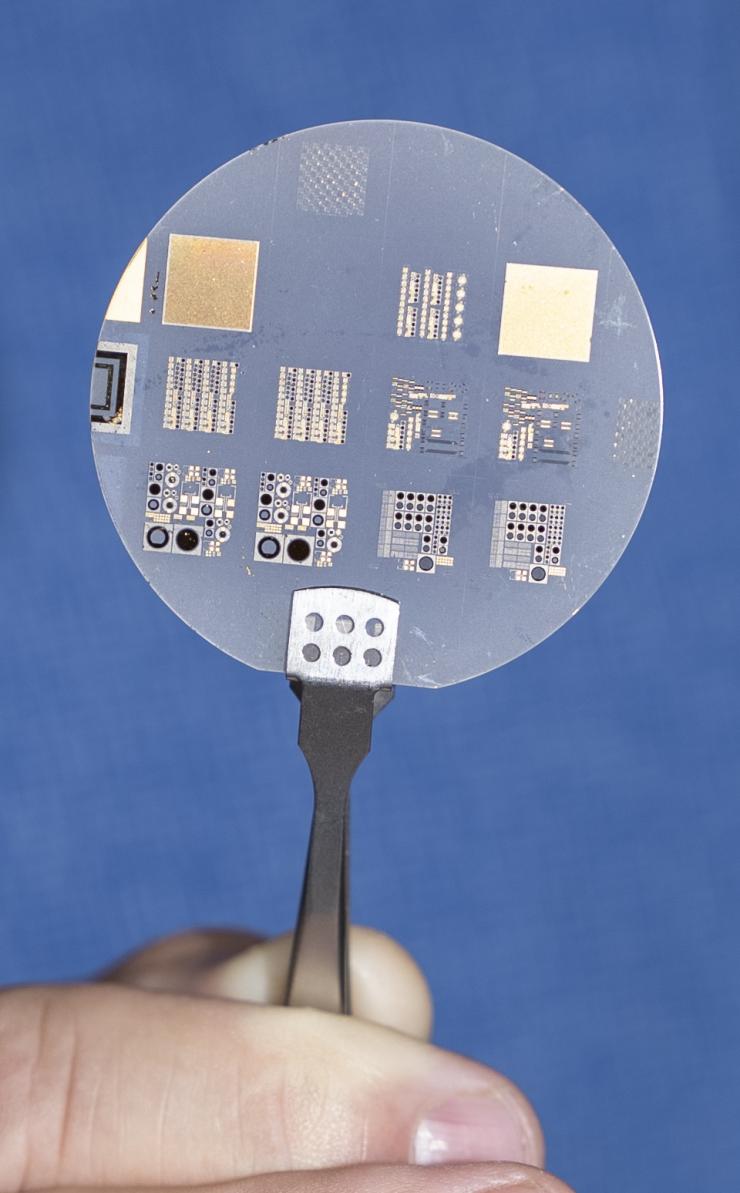
Georgia Tech’s AlN-based semiconductor has the highest bandgap ever demonstrated to have both p and n-type conduction needed for electronics.
Dan Watson
dwatson@ece.gatech.edu
Researchers 3D Print First High-Performance Nanostructured Alloy That’s Both Ultrastrong and Ductile
Aug 03, 2022 — Atlanta, GA

A strong and ductile high-entropy alloy is made from additive manufacturing, and it exhibits a hierarchical microstructure over a wide range of length scales. (Image credit: Thomas Voisin).
A team of researchers at the University of Massachusetts Amherst and the Georgia Institute of Technology has 3D printed a dual-phase, nanostructured high-entropy alloy that exceeds the strength and ductility of other state-of-the-art additively manufactured materials, which could lead to higher-performance components for applications in aerospace, medicine, energy and transportation. The research, led by Wen Chen, assistant professor of mechanical and industrial engineering at UMass, and Ting Zhu, professor of mechanical engineering at Georgia Tech, was published in the August issue of the journal Nature.
Over the past 15 years, high entropy alloys (HEAs) have become increasingly popular as a new paradigm in materials science. Comprised of five or more elements in near-equal proportions, they offer the ability to create a near-infinite number of unique combinations for alloy design. Traditional alloys, such as brass, carbon steel, stainless steel and bronze, contain a primary element combined with one or more trace elements.
Additive manufacturing, also called 3D printing, has recently emerged as a powerful approach of material development. The laser-based 3D printing can produce large temperature gradients and high cooling rates that are not readily accessible by conventional routes. However, “the potential of harnessing the combined benefits of additive manufacturing and HEAs for achieving novel properties remains largely unexplored,” says Zhu.
Chen and his team in the Multiscale Materials and Manufacturing Laboratory combined an HEA with a state-of-the-art 3D printing technique called laser powder bed fusion to develop new materials with unprecedented properties. Because the process causes materials to melt and solidify very rapidly as compared to traditional metallurgy, “you get a very different microstructure that is far-from-equilibrium” on the components created, Chen says. This microstructure looks like a net and is made of alternating layers known as face-centered cubic (FCC) and body-centered cubic (BCC) nanolamellar structures embedded in microscale eutectic colonies with random orientations. The hierarchical nanostructured HEA enables co-operative deformation of the two phases.
“This unusual microstructure’s atomic rearrangement gives rise to ultrahigh strength as well as enhanced ductility, which is uncommon, because usually strong materials tend to be brittle,” Chen says. Compared to conventional metal casting, “we got almost triple the strength and not only didn’t lose ductility, but actually increased it simultaneously,” he says. “For many applications, a combination of strength and ductility is key. Our findings are original and exciting for materials science and engineering alike.”
“The ability to produce strong and ductile HEAs means that these 3D printed materials are more robust in resisting applied deformation, which is important for lightweight structural design for enhanced mechanical efficiency and energy saving,” says Jie Ren, Chen’s Ph.D. student and first author of the paper.
Zhu’s group at Georgia Tech led the computational modeling for the research. He developed dual-phase crystal plasticity computational models to understand the mechanistic roles played by both the FCC and BCC nanolamellae and how they work together to give the material added strength and ductility.
“Our simulation results show the surprisingly high strength yet high hardening responses in the BCC nanolamellae, which are pivotal for achieving the outstanding strength-ductility synergy of our alloy. This mechanistic understanding provides an important basis for guiding the future development of 3D printed HEAs with exceptional mechanical properties,” Zhu says.
In addition, 3D printing offers a powerful tool to make geometrically complex and customized parts. In the future, harnessing 3D printing technology and the vast alloy design space of HEAs opens ample opportunities for the direct production of end-use components for biomedical and aerospace applications.
Additional research partners on the paper include Texas A&M University, the University of California Los Angeles, Rice University, and Oak Ridge and Lawrence Livermore national laboratories.
Story by Melinda Rose, Associate News Editor at UMass Amherst.
Ting Zhu, Woodruff Professor in the George W. Woodruff School of Mechanical Engineering, Georgia Institute of Technology
Catherine Barzler, Senior Research Writer/Editor
Georgia Tech Faculty and Students Win Awards, Present Research at Design Automation Conference
Jul 26, 2022 — Atlanta, GA

Members of the Georgia Tech School of Electrical and Computer were well-represented at the 59th Design Automation Conference (DAC), a premier event devoted to the design and design automation of electronic chips and systems, was held in San Francisco on July 10-14.
The 59th Design Automation Conference (DAC), a premier event devoted to the design and design automation of electronic chips and systems, was held in San Francisco on July 10-14. The conference offers training, education, exhibits, and networking opportunities for designers, researchers, tool developers and vendors. It is sponsored by the Association for Computing Machinery (ACM) and the Institute of Electrical and Electronics Engineers (IEEE), and is supported by ACM's Special Interest Group on Design Automation (SIGDA) and IEEE's Council on Electronic Design Automation (CEDA).
In the span of five days, DAC provided over 300 technical presentations and sessions that were selected by a committee of electronic design and university research experts offering information on recent developments and trends, management practices and new products, methodologies, and technologies in the electronics industry.
“DAC brings together researchers across the computing stack — technology, circuits, design-automation and computer architecture — enabling a confluence of ideas and cross-stack research," said associate professor Tushar Krishna in the Georgia Tech School of Electrical and Computer Engineering. “It provides a multitude of opportunities for researchers, students, and industry experts to collaborate and influence tomorrow’s innovations, making it a highly exciting and effective conference.”
Faculty members and students in ECE were presented with multiple awards and participated in research talks and technical sessions. ECE’s DAC awards and contributions are listed below:
Awards:
- Professor Sung Kyu Lim and his students Bon Woong Ku (currently at Synopsys) and Kyungwook Chang (currently at Sungkyunkwan University) received the 2022 Donald O. Pederson Best Paper Award for their paper “Compact-2D: A Physical Design Methodology to Build Two-Tier Gate-Level 3D ICs” published in IEEE TCAD.”
- Ph.D. candidate Poulami Das (supervised by professor Moin Qureshi) won the “Best Research Award” during the Ph.D. Forum.
- Ph.D. candidate Rishov Sarkar (supervised by assistant professor Callie Hao) won the third place in the “University Demo Best Demonstration.”
- Ph.D. candidates Foroozan Karimzadeh (supervised by ECE chair Arijit Raychowdhury), Zishen Wan (supervised by Raychowdhury), and Anurag Kar (supervised by professor Hyesoon Kim in Tech’s School of Computer Science) were named 2022 DAC Young Fellows and presented on their respective research during the DAC Young Fellows Program workshop.
Engineering Talks, Tutorials, Workshops, Panels
- Hao gave an invited talk entitled, “3U-EdgeAI: Ultra-Low Memory Training, Ultra-Low Bitwidth Quantization, and Ultra-Low Latency Acceleration” during the Fifth International Workshop on Design Automation for Cyber-Physical Systems (DACPS).”
Hao, along with Hyoukun Kwon (a recent Ph.D. graduate supervised by Krishna and now at Meta), presented the tutorial “A Journey to SW/HW Co-design in Machine Learning: Fundamental, Advancement, and Application.” They presented twice on the same day due to tutorial’s popularity.
Hao was also the co-organizer of the Early Career Workshop for junior faculty and senior Ph.D. students interested in academia.
- Krishna presented an invited talk entitled, “Formalizing Design-space Exploration for Flexible AI Accelerators” during the Silicon Integration Initiative Low-Power Forum.”
- Lim presented at the engineering track Machine Learning and EDA: The Productivity Cycle and organized the research panel “Heterogeneous 3D or Monolithic 3D, Which Direction to Go?”
Technical Sessions
- Ananda Samajdar (recent Ph.D. graduate supervised by Krishna and now at IBM) presented his work “Self-Adaptive Reconfigurable Arrays (SARA): Learning Flexible GEMM Accelerator Configuration and Mapping-space using ML.”
- Ph.D. candidate Brian Crafton (supervised by Raychowdhury) presented his work “Improving Compute In-Memory ECC Reliability with Successive Correction”.
- Hao presented her work “H2H: Heterogeneous Model to Heterogeneous System Mapping with Computation and Communication Awareness”.
Learn more about the Design Automation Conference

L-R: Zishen Wan (Ph.D. candidate), Callie Hao (assistant professor), Rishov Sarkar (Ph.D. candidate), Poulami Das (Ph.D. candidate), and Anurag Kar (Ph.D. candidate) all won awards at DAC.

Ph.D. candidate Rishov Sarkar (right) won third place in “University Demo Best Demonstration.” He is supervised by ECE assistant professor Callie Hao (left).

ECE assistant professor Callie Hao presenting the popular tutorial “A Journey to SW/HW Co-design in Machine Learning: Fundamental, Advancement, and Application.”
 and his former student Bon Woong Ku (middle) receiving the 2022 Donald O. Pederson Best Paper Award")
Professor Sung Kyu Lim (right) and his former student Bon Woong Ku (middle) receiving the 2022 Donald O. Pederson Best Paper Award for their paper “Compact-2D: A Physical Design Methodology to Build Two-Tier Gate-Level 3D ICs” published in IEEE TCAD.”

Ph.D. candidate Poulami Das won the “Best Research Award” during the Ph.D. Forum at DAC.
Dan Watson
dwatson@ece.gatech.edu
IEN Networking Lunch
Calling all researchers!
All Georgia Tech faculty and researchers are invited to join leaders from the Institute for Electronics and Nanotechnology (IEN) and their colleagues from across campus for an informal, no-host networking lunch. This is a great opportunity to learn more about IEN, its research areas, and potential partnership opportunities.
IEN Networking Lunch
Calling all researchers!
All Georgia Tech faculty and researchers are invited to join leaders from the Institute for Electronics and Nanotechnology (IEN) and their colleagues from across campus for informal, no-host networking lunches. These are a great opportunity to learn more about IEN, its research areas, and potential partnership opportunities.