$65M Grant to Build AI Manufacturing in Georgia
Sep 06, 2022 — Atlanta, GA
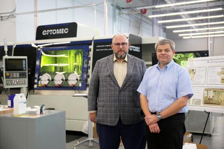
Aaron Stebner (left) and Tom Kurfess are among the leaders of GA-AIM, a $65 million grant that focuses on manufacturing and AI in the state of Georgia.
Aaron Stebner outlined an aggressive plan for artificial intelligence and manufacturing when he applied for a faculty position in 2019. In his cover letter, he promised “to establish the Georgia Institute of Technology as a world leader in additive manufacturing of solid materials (ceramics & metals) R&D, especially in the fusion of data sciences and AI to create new, world-leading technologies.”
Stebner thought it would take 10-15 years of incremental steps and funding to achieve the goal. He was wrong.
Thanks to a new $65 million grant from the U.S. Department of Commerce’s Economic Development Administration, announced by President Joe Biden, Stebner’s plan will begin to become a reality — and include the entire state of Georgia and all of its manufacturing sectors from agriculture to airplanes — two years after arriving on campus.
The largest of the nine projects within the larger Georgia AI Manufacturing (GA-AIM) technology corridor grant will allow Stebner and Georgia Tech to transform the Advanced Manufacturing Pilot Facility (AMPF) into the Artificial Intelligence Manufacturing Pilot Facility (AI-MPF). The 24,000 square-foot facility on 14th Street will more than double in size after Georgia Tech and statewide GA-AIM partners were selected as one of 21 Phase II awardees in the $1 billion Build Back Better Regional Challenge (BBB) competition, part of the Investing in America’s Communities initiative under the American Rescue Plan Act of 2021.
AMPF has been a shell waiting for a vision like Build Back Better to fill it out,” said Stebner, associate professor the George W. Woodruff School of Mechanical Engineering and the School of Materials Science and Engineering. “Now we will transform the facility into one of the nation’s first manufacturing labs designed for autonomy with the goal of helping the state and the nation to be world AI manufacturing leaders.”
Read the entire story on the College of Engineering website.
Jason Maderer
College of Engineering
maderer@gatech.edu
2022-2023 Georgia Tech Institute for Electronics and Nanotechnology (IEN) Core Facilities Seed Grant Program
Sep 02, 2022 — Atlanta, GA
IEN Seed Grant logo
Program Description
The Georgia Tech IEN is an Interdisciplinary Research Institute (IRI) comprised of faculty and students interested in using the most advanced facilities for fabrication, characterization, and cleanroom processes, to facilitate research in micro- and nano-scale materials, devices, and systems. Applications of this research span all disciplines in science and engineering with particular emphasis on biomedicine, electronics, optoelectronics and photonics, and energy applications. As there can be a learning curve associated with initial proof-of-concept development and testing using cleanroom tools, this seed grant program was developed to expedite the initiation of new graduate students and new research projects into productive activity. Successful proposals to this program will identify a new, currently-unfunded research idea that requires core facility access to generate preliminary data necessary to pursue other funding avenues.
Program Eligibility
This program is open to any current Georgia Tech or GTRI faculty member as project PI. The graduate student performing the research should be in the first 2 years of their graduate studies, and preference will be given to students who are new users of the IEN facilities. The student’s research advisor (project PI) does not need to be a current user of the IEN cleanroom/lab facilities. Current PI awardees cannot apply in consecutive funding periods. Please make sure that the student will be available to use the facility during the majority of the grant period.
Award Information
Each seed grant award will consist of free core facility access to the student identified in the proposal over a 12-month period (4 consecutive billing quarters) up to a maximum of $6600 in charges. This award amount is based on the current access rates and the academic cap on quarterly charges and equates to two free billing quarters spread over one year in order to provide maximum flexibility in access. This maximum amount is subject to change based on planned access rate adjustments. This maximum award amount is still in effect even if IEN non-cleanroom (lab) equipment, electron beam lithography (EBL), or tools in the Materials Characterization Facility (MCF) are required. Access to facilities other than IEN/MCF are not covered by the seed grant.
In addition, each student will be offered up to $500 in travel support to attend a scientific conference where they will present (oral or poster) the work resulting from this seed grant. This travel can be used during the award period or up to a period of 6 months following.
The number of awards for each proposal submission cycle will depend on the number and quality of the proposals.
Expectations
The seed grant will begin with a group kickoff meeting (mandatory for students) with IEN technical staff and will also include periodic check-in meetings as required. Members of the IEN processing staff will also be available to consult as needed during the project period. The designated student user is expected to only utilize the seed grant for core facility access while working with the PI on the proposed project. A short progress report is submitted at the mid-point of the project, and a longer report describing the research activities and outcomes is required at the completion of the award period. Students may also be requested to present a poster at the annual IEN User Day event.
Submission Schedule
This Seed Grant program is offered in two competitions each year with due dates this academic year on October 1, 2022 and April 1, 2023 for research activity that will begin on December 1, 2022 and June 1, 2023, respectively.
Proposal Requirements (2 pages max)
The proposal (submitted as a PDF file of no more than 2 pages) should do the following:
1. Provide a project title. List name of faculty PI and student at the top of the proposal.
2. Identify the research problem and specify the proposed methods.
3. Indicate the IEN research tools necessary to conduct the research. It is recommended that you obtain assistance with this component from members of the IEN or MCF technical staff.
4. Describe the relationship of this research to the PI’s other research activity and how it is distinct from and not an extension of ongoing work.
5. Identify the PI and the graduate student involved (including year of graduate work), and if there will be a mentoring relationship with the PI’s other students. Note if there are collaborative relationships with Georgia Tech faculty that bear on this research project.
6. Specify the potential for follow-on funding based on the results of this initial work.
Some helpful hints: Proposals should not excessively discuss the motivation and impact of the research. While this is helpful for understanding the importance of the work, please be brief. More important is a detailed description of what you propose to actually do (fabrication and/or characterization) in the core facilities so that this can be assessed for how feasible and realistic it is within the scope of IEN’s capabilities. We understand that this research is being undertaken by a beginning graduate student with limited experience who will likely require staff assistance. In addition, there may be multiple approaches
to the research problem. However, you should clearly describe at least the most promising approach in detail within the page limitations.
Submit the PDF file by the specified due date to Ms. Amy Duke (amy.duke@ien.gatech.edu).
Review Criteria
Proposals will initially be reviewed by IEN staff for technical feasibility within the time frame. Rating of proposals will be done by a review committee of Georgia Tech faculty, with final selection of awardees by IEN staff. Review criteria include novelty of the research, clarity of the proposed work, work that is technically achievable within the time constraints, and likelihood of positive outcomes (future funding).
For more information, please contact Dr. David Gottfried, dsgottfried@gatech.edu, (404) 955-9733.
Dr. David Gottfried, dsgottfried@gatech.edu, (404) 955-9733.
Economic Development Administration Awards Georgia Tech $65 Million for AI Manufacturing Project
Sep 02, 2022 — Atlanta, GA

Georgia Tech is developing plans with partners across the state to build the Georgia Artificial Intelligence Manufacturing Corridor (GA-AIM). This project aims to build and bolster Georgia's economy by filling existing technology gaps, building a technological opportunity framework that includes underrepresented communities and rural Georgia counties, and better securing the state’s manufacturing infrastructure.
The Georgia Institute of Technology has been awarded a $65 million grant from the U.S. Department of Commerce’s Economic Development Administration (EDA) to support a statewide initiative that combines artificial intelligence and manufacturing innovations with transformational workforce and outreach programs. The grant will increase job and wage opportunities in distressed and rural communities, as well as among historically underrepresented and underserved groups.
The Georgia Artificial Intelligence Manufacturing Technology Corridor (GA-AIM) effort is one of 21 winning projects the White House announced today under the Biden administration’s $1 billion Build Back Better Regional Challenge. The award follows a $500,000 Phase 1 feasibility grant the project received in 2021.
“Georgia Tech is honored to lead this vision of collaborative innovation and economic development across all regions of our state,” said Georgia Tech President Ángel Cabrera. “This award underscores the Institute's commitment to leverage our resources and expertise to address great challenges, serve our state and nation, and amplify our impact on the world.”
The selected awardees represent projects in 24 states with grant amounts ranging from $25 million to $65 million.
“As we invest and grow critical industries in the U.S., we want to create industry hubs in diverse communities across the country,” U.S. Secretary of Commerce Gina Raimondo said in a statement. “These grants will provide critical and historic funding directly to community coalitions to invest in new infrastructure, research and development, and workforce development programs while creating good-paying jobs, supporting workers, and prioritizing equity.”
The GA-AIM project is led by Aaron Stebner, associate professor in the George W. Woodruff School of Mechanical Engineering and the School of Materials Science and Engineering; Donna Ennis, director of Diversity Engagement and Program Development in Georgia Tech’s Enterprise Innovation Institute and also director of its Georgia MBDA Business Center; and Thomas R. Kurfess, executive director of the Georgia Tech Manufacturing Institute.
“The ability to integrate our discoveries and innovations here at the AI Manufacturing Pilot Facility with novel workforce programs and transformative outreach experiences is a once-in-a-lifetime opportunity to do something greater in ways that increase opportunity and prosperity for all Georgians,” Stebner said. “Through an equitable AI manufacturing innovation focus, the assembled coalition of partners and stakeholders across the state will build a more prosperous and resilient Georgia and set a nation-leading example.”
The AI Manufacturing Pilot Facility, which will allow for government and industry pilot trials, cybersecurity games, and workforce training for AI manufacturing technologies, is just one component of Georgia Tech’s support for the project.
Two of Georgia Tech’s commercialization programs — VentureLab and I-Corps South — will create a center for the commercialization of AI manufacturing technologies into local and regional startups through training built on the National Science Foundation’s I-Corps curriculum.
The Enterprise Innovation Institute, Georgia Tech’s economic development arm, will engage in focused outreach and technical assistance to small- and mid-sized manufacturers and minority business enterprises through its Georgia Manufacturing Extension Partnership (GaMEP) and Georgia MBDA Business Center programs. Other Enterprise Innovation Institute programs include the Economic Development Lab, the Partnership for Inclusive Innovation, and ATDC, which will focus on outreach and engagement in distressed and underserved parts of the state, create workforce development programs, implementation strategies, and attract outside investment.
“The work that we will accomplish with our broad spectrum of partners in this new endeavor will leverage the latest technology in artificial intelligence to grow and strengthen our workforce ensuring that the growing manufacturing sector in Georgia has the skilled workforce that it requires for today’s as well as tomorrow’s needs,” Kurfess said. “At the same the high paying and secure jobs will be going to a very diverse population base from across the state, providing an equitable robust future for all citizens of Georgia.”
Georgia Tech’s Supply Chain & Logistics Institute will study the impact of automation technologies, build automation solutions tailored for rural manufacturers, and create programs that lower the barrier for rural manufacturers’ access to use the AI Manufacturing Pilot Facility.
In addition, Georgia Tech’s Ethics, Technology, and Human Interaction Center (ETHICx), led by faculty in the Ivan Allen College of Liberal Arts, will help integrate considerations of equity, fairness, accountability, and transparency into GA-AIM and promote the responsible and ethical use of AI-manufacturing technologies.
Finally, Georgia Tech’s K-12 InVenture Prize and Center for Education Integrating Science, Mathematics and Computing programs will expand their emphasis to rural and underserved areas of the state by piloting a rural regional event with a region-specific prize. They will also create supplemental lessons centered on AI and data science that will be part of a K-12 InVenture Prize curriculum website.
“We are excited to be a part of this collaborative effort to catalyze research and innovation in AI and manufacturing across the state of Georgia,” said Chaouki T. Abdallah, executive vice president for Research at Georgia Tech. “This project aligns with our goals to expand economic opportunity in our state's underserved communities, and to serve as a collaborative hub for interdisciplinary research that advances technology and improves people’s lives.”
Georgia Tech is working with a coalition of statewide partners to create a foundation that supports existing business growth and new business ventures across the state especially in underserved communities and rural Georgia.
“All across the state of Georgia, our programs in the Enterprise Innovation Institute work hard to unlock potential and foster economic opportunity for all, particularly in underserved and marginalized communities,” said David Bridges, vice president of the Enterprise Innovation Institute, and co-author of the grant proposal with Stebner. “This project leverages what we and our partners each do best to help achieve our broader Georgia AIM goals.”
Tech’s partners include the:
· Georgia Department of Community Affairs
· Houston County Development Authority
· KITTLabs
· Russell Innovation Center for Entrepreneurs
· Robins Air Force Base 21st Century Partnership
· Southwest Georgia Regional Commission
· Technology Association of Georgia Education Collaborative
· Technical College System of Georgia
“What's really special about this effort is that it's centered on a wholistic approach with innovation, not just one piece of AI or manufacturing,” Ennis said. “We're working collectively statewide to transform and propel forward our industry, communities, and most importantly, our people.”
That collective approach is critical to GA-AIM’s success, said Houston County Development Authority Executive Director Angie Gheesling.
“The Development Authority and the 21st Century Partnership lead the Middle Georgia Innovation Project, which includes 11 counties in the Middle Georgia region, a diverse landscape of communities from rural to urban,” she said. “This award further facilitates the continuation of several years of collaboration between local leadership, our universities, private industry, and Robins Air Force Base to position ourselves as a Software Center of Excellence. We are grateful to Georgia Tech for the opportunity to partner and contribute to the overall future success of GA-AIM.”
Burunda Prince, chief operating officer of the Russell Innovation Center for Entrepreneurs, echoed those sentiments, saying its reach is exponentially amplified through the GA-AIM partnership.
The Center will create a mobile, 5,000-square-foot LaunchPad AI Innovation Studio to provide prototyping and proof-of-concept development of physical products. Black entrepreneurs in rural and urban Georgia will have access to equipment, training, and mentoring, and LaunchPad AI will also be open to AI InVenture teams from Atlanta’s urban K-12 schools.
“As part of the Build Back Better grant, the Russell Innovation Center for Entrepreneurs will help Black businesses leverage the benefits of artificial intelligence to provide better data and insights that will build stronger companies and drive greater wealth generation,” Prince said. “What makes this opportunity unique is the cross collaboration of partners which will engage and empower communities across Georgia through access to technologies that often are inaccessible.”
Equally as important is the education component and the ability for it to be a bridge to new skills and opportunities for Georgia workers, said Technical College System of Georgia Commissioner Greg Dozier.
“The funding for the project will equip four TCSG colleges with state-of-the-art manufacturing studios that will showcase the clean, safe state of modern manufacturing,” Dozier said. “Automation in manufacturing creates a demand for more skilled jobs, giving TCSG the charge to strengthen the workforce pipeline by training Georgians in these exciting, new technologies. The Georgia AIM project provides the funding to meet these opportunities head on.”
###
About the U.S. Economic Development Administration
The mission of the U.S. Economic Development Administration (EDA) is to lead the federal economic development agenda by promoting competitiveness and preparing the nation's regions for growth and success in the worldwide economy. An agency within the U.S. Department of Commerce, EDA makes investments in economically distressed communities to create jobs for U.S. workers, promote American innovation, and accelerate long-term sustainable economic growth.
About the Georgia Institute of Technology
The Georgia Institute of Technology, or Georgia Tech, is a top 10 public research university developing leaders who advance technology and improve the human condition. The Institute offers business, computing, design, engineering, liberal arts, and sciences degrees. Its nearly 44,000 students representing 50 states and 149 countries, study at the main campus in Atlanta, at campuses in France and China, and through distance and online learning. As a leading technological university, Georgia Tech is an engine of economic development for Georgia, the Southeast, and the nation, conducting more than $1 billion in research annually for government, industry, and society.
Writer: Péralte C. Paul I peralte.paul@comm.gatech.edu I 404.316.1210
Media contact: Ayana Isles | aisles3@gatech.edu | 404.660.2927
GLUE Webinar: General Lectures Uniting Everyone
This webinar is offered virtually via Zoom. Please click here to register.
"Bringing Engineers & Clinicians Together To Explore Microchip Applications In Healthcare"
Farrokh Ayazi, Ph.D.
Regents Entrepreneur & Ken Byers Professor in Microsystems
School of Electrical and Computer Engineering
Georgia Tech
Lim Becomes First ECE Faculty Member to Join DARPA as Program Manager
Aug 31, 2022 — Atlanta, GA

ECE Professor Sung-Kyu Lim
This August, Georgia Tech professor Sung Kyu Lim joined the Defense Advanced Research Projects Agency (DARPA) as a program manager in the Microsystems Technology Office (MTO). Lim, the Motorola Solutions Foundation Professor in School of Electrical and Computer Engineering (ECE), is the first Georgia Tech ECE researcher to be recruited and serve as a DARPA program manager while teaching at Georgia Tech.
As a prominent researcher in very-large-scale integration (VLSI) systems and design, Lim’s first program at DARPA, dubbed the “3D-EDA (3D Electronic Design Automation) Program,” will develop heterogeneous 3D integrated circuits (IC) design and simulation software to automatically co-optimize the underlying device, circuit, and architecture. The program will use 3D-EDA tools to demonstrate 10x shorter design turnaround time and 10x energy-efficiency improvement.
“We are very proud of Sung Kyu’s appointment to DARPA’s Microsystems Technology Office,” said Arijit Raychowdhury, ECE’s Steve W. Chaddick School Chair. “This is an important recognition of Sung Kyu’s standing in the VLSI field, and also shows how Georgia Tech ECE researchers are leading, on the national level, in developing advanced defense research projects.”
The core mission of DARPA’s MTO is to develop high-performance intelligent microsystems and next-generation components to ensure U.S. dominance in the areas of Command, Control, Communications, Computing, Intelligence, Surveillance, and Reconnaissance (C4ISR), Electronic Warfare (EW), and Directed Energy (DE).
According to DARPA, the office’s work in applying advanced capabilities in areas such as wide-band gap materials, phased array radars, high-energy lasers, complementary metal-oxide-semiconductor (CMOS) circuits, and infrared imaging has helped the U.S. establish and maintain technological superiority for more than two decades.
Lim’s DARPA assignment is supported by the U.S. Department of Defense’s (DoD) Intergovernmental Personnel Act (IPA), which allows for the temporary assignment of skilled personnel between the Federal Government and state and local governments, colleges and universities, Indian tribal governments, federally funded research and development centers, and other eligible organizations.
He will serve for four years at the agency in Washington D.C. before returning to Georgia Tech. Lim’s GTCAD (Georgia Tech Computer-Aided Design) Lab will remain open during his 4-year DARPA term.
Dan Watson
dwatson@ece.gatech.edu
2022-2023 Institute for Bioengineering and Bioscience Distinguished Lecture
"Designer Nanocarriers for Cancer Therapy"
Paula T. Hammond, Ph.D.
Institute Professor and Department Head of Chemical Engineering
Koch Institute of Integrative Cancer Research
Massachusetts Institute of Technology
Exponential Electronics Proposers Mini-Workshop
Institute for Electronics and Nanotechnology Exponential Electronics (IEN-EX) Proposers Mini-Workshop
Potential IEN-EXproposers are encouraged to attend the mini-workshop on September 15, 2022, from 11:00 a.m. - 1:00 p.m. in Marcus 1117/1118. Michael Filler, IEN Associate Director for Research Programs, will explain the motivation and goals of the IEN-EX program, provide examples of 1000x ideas, as well as offer attendees time to discuss potential 1000x ideas and begin team building.
Tech Faculty Tapped for Regents' Awards
Aug 11, 2022 — Atlanta, GA

Koan at Georgia Tech
Along with the Georgia Tech faculty tapped and reappointed as Regents’ Professors and Researchers at the Aug. 9 University System of Georgia (USG) Board of Regents meeting were five Georgia Tech professors named to the new distinction of Regents’ Entrepreneur.
Georgia Tech faculty named as the first Regents' Entrepreneurs in the USG include Farrokh Ayazi, Ken Byers Professor in Microsystems, School of Electrical and Computer Engineering; Kirk Bowman, professor, Sam Nunn School of International Affairs; Andrei Fedorov, Neely Chair and professor, Woodruff School of Mechanical Engineering and the Petit Institute for Bioengineering and Biosciences; Mark Prausnitz, Regents’ Professor, J. Erskine Love Jr. Chair, School of Chemical and Biomolecular Engineering; and Gleb Yushin, professor, School of Materials Science and Engineering.
Regents’ Professor First-Time Appointments
The Board of Regents approved the title of Regents’ Professor to Facundo Fernández, professor and Vasser Woolley Foundation Chair in Bioanalytical Chemistry, School of Chemistry and Biochemistry; Willie Pearson, professor of sociology, School of History and Sociology; Krishnendu Roy, professor, Robert A. Milton Endowed Chair, NSF Engineering Research Center for Cell Manufacturing Technologies, Coulter Department of Biomedical Engineering; and Beril Toktay, professor of Operations Management and Brady Family Chairholder, Scheller College of Business.
Regents’ Researcher First-Time Appointments
Those named as Regents’ Researchers include Stephen Balakirsky, principal research scientist, Georgia Tech Research Institute (GTRI); Anton Bryksin, principal research scientist, Petit Institute for Bioengineering and Bioscience; Walter Bradley Fain, principal research scientist, School of Public Policy; and Anita Pavadore, principal research engineer, GTRI.
First-Time Reappointments
Receiving a first-time reappointment as Regents’ Professor was Surya Kalidindi, Regents’ Professor, Rae S. and Frank H. Neely Chair, Woodruff School of Mechanical Engineering. Receiving a first-time reappointment as Regents’ Researcher was Margaret Loper, principal research scientist, GTRI.
Other Reappointments
Regents’ Professor and Researcher designations only require Institute approval for second-time reappointments. Second-time Regents’ Professor appointments at Georgia Tech include Sy Goodman, Regents’ Professor and professor of International Affairs and Computing, Sam Nunn School of International Affairs; Nicholas Hud, Regents’ Professor, School of Chemistry and Biochemistry; and Vladimir Tsukruk, Regents’ Professor, School of Materials Science and Engineering. Receiving a second-time Regents’ Researcher reappointment was Alexa Harter, director of the Cybersecurity, Information Protection, and Hardware Evaluation Research Laboratory at GTRI.
New Recognition for Entrepreneurship and Innovation
The board approved the Regents’ Entrepreneur designation in their February 2022 meeting to recognize and support faculty entrepreneurship and innovation. The Regents’ Entrepreneur designation may be granted by the Board of Regents to an outstanding full-time tenured faculty member who has an established reputation as a successful innovator and who has taken their research into a commercial setting. The Regents’ Entrepreneur designation is bestowed by the board only upon the unanimous recommendation of the USG institution president, the chief academic officer, and the chancellor, and upon the approval of the Committee on Academic Affairs.
Farrokh Ayazi
Farrokh Ayazi is director of the Georgia Tech Analog Consortium. His main research interest is in integrated micro and nano electromechanical systems and integrated microsystem design. He is the founder and chief technology officer of Qualtré, which was acquired by Panasonic in 2016. He is currently leading StethX Microsystems, an ATDC company, in commercializing advanced wearable sensors for cardiopulmonary applications.
Kirk Bowman
Kirk Bowman is the Rise Up & Care term chair in Global Development and Identity. In 2014, Bowman founded Rise Up & Care, a nonprofit corporation that employs an innovative model of international community development, combining global development research; high-level performance organizations in the Global South to transform youth; powerful documentary films by top local directors; and children's books illustrated by local street artists. He directs a Georgia Tech Vertically Integrated Project on Global Social Entrepreneurship with 18 undergraduate students.
Andrei G. Fedorov
Andrei G. Fedorov’s research covers atomic scale nanomanufacturing; distributed power generation with carbon dioxide management; instrumentation for biomedical research; and thermal management of electronics and medicine. With his students and collaborators, Fedorov started several technology companies to commercialize his inventions in the space of gene/drug delivery; biomarker discovery and quality control in cell therapy manufacturing; and thermal management of high-power generation devices.
Mark Prausnitz
Mark Prausnitz has co-founded seven companies that have together raised more than $350 million for commercialization of microneedle technologies developed in his lab at Georgia Tech. Three of the companies have products for sale, including an FDA-approved treatment of ocular inflammation. His technologies have been studied in more than 20 human clinical trials. He has almost 80 issued or pending U.S. patents, with additional international filings. Prausnitz has published more than 300 journal articles and supervised 50 Ph.D. students among a total of almost 350 graduate, postdoctoral, or undergraduate researchers in his lab.
Gleb Yushin
Gleb Yushin is a pioneer and globally recognized leader in advanced materials for next-generation Li-ion batteries. He is member of the National Academy of Inventors and fellow of three international professional societies. He has been awarded more than 200 patents, while also being one of the most cited Georgia Tech professors since 2019. He co-founded the most economically successful Georgia Tech startup Sila Nanotechnologies ($3.3B valuation). Yushin has served as a founding faculty advisor for the Entrepreneurs Club at Tech and as an advisor to the Georgia Tech startup CellFE.
Regents’ Professorships and Regents’ Researcher titles may be granted for a period of three years by the Board of Regents to outstanding faculty members of Georgia Tech, Augusta University, Georgia State University, the University of Georgia, and, in special circumstances, other USG institutions.
Dawn Baunach, Associate Vice Provost for Faculty
New Chip Could Make Treating Metastatic Cancer Easier and Faster
Aug 11, 2022 — Atlanta, GA

Fabrication of the microchip. The device is fabricated by injecting a polymer into a micro fabricated mold and the polymer is cured under ultraviolet light to produce low-cost, single-use devices.
Cancer spreads via circulating tumor cells (CTCs) that travel through the blood to other organs, and they are nearly impossible to track. Now, researchers at the Georgia Institute of Technology have found a detection method that could revolutionize cancer treatment by showing how cancers metastasize and what stage they are. This could lead to earlier and more targeted treatment, beginning with a simple blood test.
When a tumor starts metastasizing, it sheds its cell into the blood. An individual cell often doesn’t survive the bloodstream on its own, but clusters of cells are much more robust and can travel to other organs, effectively pushing the cancer to a metastatic state.
CTCs have proven difficult to study, let alone treat. Blood contains billions of cells per milliliter, and only a handful of those cells would be CTCs in a patient with metastatic cancer. Such intense filtration has been inaccessible using conventional lab methods. Most traditional filtration is too aggressive and would break the cluster back into single cells and ruin the ability to study the effect of a cluster.
“That’s what got engineers like me interested in this because we are really good at creating sensors, or small devices that actually do sensitive analysis,” said School of Electrical and Computer Engineering Associate Professor Fatih Sarioglu. “We started developing technologies to catch these precious cells to help manage cancer better.”
Sarioglu presented the research in “High Throughput, Label-free Isolation of Circulating Tumor Cell Clusters in Meshed Microwells,” recently published in Nature Communications.
Creating the Cluster-Well
Sarioglu’s lab invented a new type of chip called the Cluster-Well, combining the precision of microfluidic chips with the efficiency of membrane filtration to find CTC clusters. Using micron-sized features, microfluidic chips can precisely locate each cell in a blood sample and determine if it’s cancerous.
“Microfluidic chips give you more control as a designer to actually ask whatever question that you want to ask those cells,” Sarioglu said. “It increases the precision and sensitivity, which is what you need for an application like this because you want to find that single cell out of many blood cells.”
To rapidly process a clinically relevant volume of blood, the researchers relied on membrane filtration to make the chip operation more scalable. In effect, the chip looks like a standard membrane filter, but under an electron microscope the microfluidic chip reveals its delicate structure used to capture clusters while letting other blood cells pass through.
Practicality was just as important as functionality to the researchers. Although the chip is initially fabricated with silicon just like a central processing unit in a computer, it is later transferred to polymers to make it accessible, affordable, and single-use, while still retaining its delicacy and precision.
“We really created only the traps that we need to have for recognizing the clusters with the microfluidic chip, and the rest is just a standard filter holder,” Sarioglu said. “Compared to a conventional microfluidic chip, you will get a much more practical assay with orders of magnitude improvement in throughput and a higher sensitivity.”
Analyzing Patient Tumor Cell Clusters
The researchers used the chip to screen blood samples from patients with ovarian or prostate cancers through a partnership with the Emory and Northside Hospitals. They isolated CTC clusters ranging from two to 100 or more cells from prostate and ovarian cancer patients and used RNA sequencing to analyze a subset.
The chip’s unique design means CTC clusters are filtered in microwells and can later be accessed for further analysis. Even a single CTC can contain a significant amount of data on the patient and their specific cancer, which can be critical for managing the disease. For example, the researchers noted hundreds of CTCs in clusters in the blood of ovarian cancer patients, some still alive, a finding that could be consequential to the spread of the disease.
Also, by sequencing the RNA in prostate CTC clusters isolated by the chip, the researchers identified specific genes expressed by these metastasizing cells. Importantly, CTC clusters from different patients were shown to express different genes, which can be potentially utilized to develop personalized, targeted therapies. Sarioglu envisions Cluster-Wells as being a routine part of the treatment process to determine what stage the cancer is at from a simple blood draw.
“Finding these clusters was very elusive,” Sarioglu said. “But this is a technology that allows these precious circulating tumor cell clusters virtually in any cancer to be accessed with precision and practicality that has not been possible before.”
CITATION: Boya, M., Ozkaya-Ahmadov, T., Swain, B.E. et al. High throughput, label-free isolation of circulating tumor cell clusters in meshed microwells. Nat Commun 13, 3385 (2022). https://doi.org/10.1038/s41467-022-31009-9
A circulating tumor cell cluster isolated from a prostate cancer patient blood sample is being imaged with a fluorescence microscope. Tumor cells are labeled with a green fluorescent label for identification.
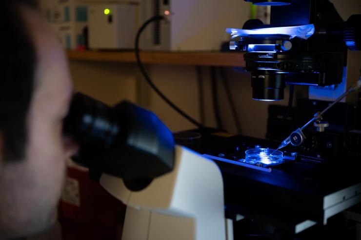
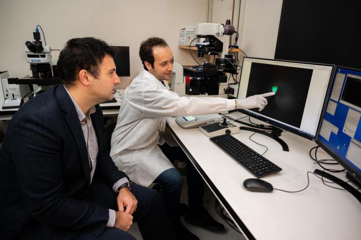
Tumor cells harvested from patient blood samples are being picked from the device for sequencing. The device is in a Petri dish on the microscope stage. A glass micro capillary collects the circulating tumor cell clusters.
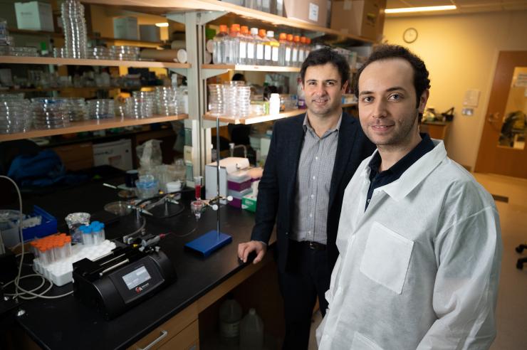
Prof. A. Fatih Sarioglu (front) and the graduate student Mert Boya are near the instrumental setup used to process the patient blood samples.
Tess Malone, Research Writer/Editor
Top Prize Awarded to Lim, Agnesina for 3D IC Design Methodology Research
Aug 11, 2022 — Atlanta, GA
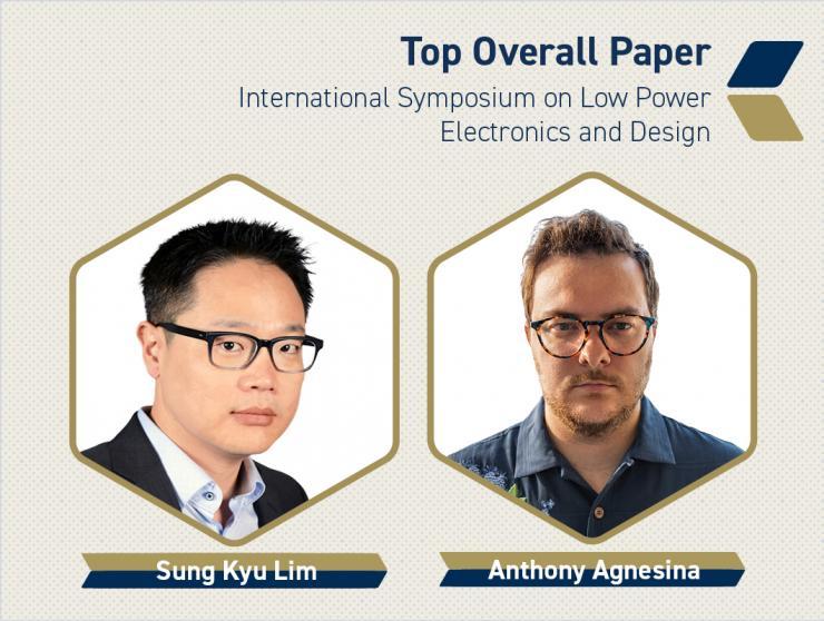
Georgia Tech professor Sung Kyu Lim and recent Ph.D. graduate Anthony Agnesina
The award-winning article proposes a novel hierarchical physical design flow enabling the building of high-density and commercial-quality two-tier face-to-face-bonded hierarchical 3D ICs.
Georgia Tech professor Sung Kyu Lim and recent Ph.D. graduate Anthony Agnesina have won the top paper award at the 2022 International Symposium on Low Power Electronics and Design (ISLPED) for their research entitled, “Hier-3D: A Hier archical Physical Design Methodology for Face-to-Face-Bonded 3D ICs.”
Lim is a Motorola Solutions Foundation Professor in Tech’s School of Electrical and Computer Engineering (ECE) and Agnesina is currently a research scientist at NVIDIA and was advised by Lim while at Georgia Tech. Co-authors include eight researchers from the Interuniversity Microelectronics Centre (IMEC), the University of Bremen, ETH Zurich, and the University of Bologna.
The award-winning article proposes a novel hierarchical physical design flow enabling the building of high-density and commercial-quality two-tier face-to-face-bonded hierarchical 3D ICs. Hierarchical very-large-scale integration (VLSI) flows are an understudied yet critical approach to achieving design closure at giga-scale complexity and gigahertz frequency targets.
The authors significantly reduced the associated manufacturing cost compared to existing 3D IC implementation flows and, for the first time, achieved cost competitiveness against the 2D reference in large modern designs.
Experimental results on complex industrial and open manycore processors demonstrate in two advanced nodes that the proposed flow provides major power, performance, and area/cost (PPAC) improvements of 1.2 to 2.2× compared with commercial 2D ICs, where all metrics are improved simultaneously, including up to 20% power savings.
ISLPED was held at the Boston University Electrical and Computer Engineering Department / Photonics Center on August 1-2, 2022. The symposium is the premier forum for presentation of innovative research in all aspects of low power electronics and design, ranging from process technologies and analog/digital circuits, simulation and synthesis tools, system-level design, and optimization, to system software and applications.
Dan Watson
dwatson@ece.gatech.edu