Nano@Tech Spring 2023 Series | LEEFT with Nano for Water Disinfection
Featuring Xing Xie, Assistant Professor and Carlton S. Wilder Junior Professor School of Civil and Environmental Engineering, Georgia Tech
Abstract: Water is a basic human need. Nevertheless, more than 10% of the world’s population lacks access to safe drinking water. An effective water disinfection method is still not readily accessible to these people. In developed urban areas, water is typically disinfected in a centralized facility through chlorine-based methods that inevitably generates harmful disinfection byproducts.
Distinguished Lecture in Materials (Virtual) | Applications of and advances in Boron Nitride Nanotubes and Additively Manufactured Ceramic Matrix Composites
Featuring Ryan Holtschneider, Lead Data Scientist at Epic Advanced Materials
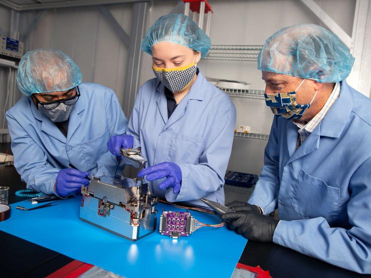
Georgia Tech Battery Day
Convening Georgia Tech and Industry to Advance Energy Storage Technologies
To view the agenda and registration information, visit the Battery Day website at: research.gatech.edu/georgia-tech-battery-day
Fall 2022 IEN Seed Grant Winners Announced
Jan 05, 2023 — Atlanta, GA

The Institute for Electronics and Nanotechnology (IEN) at Georgia Tech has announced the Fall 2022 Core Facility Seed Grant winners. The primary purpose of this program is to give first- and second-year graduate students in diverse disciplines working on original and unfunded research in micro- and nanoscale projects the opportunity to access the most advanced academic cleanroom space in the Southeast. In addition to accessing the labs' high-level fabrication, lithography, and characterization tools, the awardees will have the opportunity to gain proficiency in cleanroom and tool methodology and access the consultation services provided by research staff members in IEN. Seed Grant awardees are also provided travel support to present their research at a scientific conference.
In addition to student research skill development, this biannual grant program gives faculty with novel research topics the ability to develop preliminary data to pursue follow-up funding sources. The Core Facility Seed Grant program is supported by the Southeastern Nanotechnology Infrastructure Corridor (SENIC), a member of the National Science Foundation’s National Nanotechnology Coordinated Infrastructure (NNCI).
Since the start of the grant program in 2014, 82 projects from ten different schools in Georgia Tech’s Colleges of Engineering and Science, as well as the Georgia Tech Research Institute and three other universities, have been seeded.
The four winning projects in this round were awarded IEN cleanroom and lab access time to be used over the next year. In keeping with the interdisciplinary mission of IEN, the projects that will be enabled by the grants include research in microelectronics, optoelectronics, battery technology, and novel materials for energy harvesting.
The Fall 2022 IEN Core Facility Seed Grant Award winners are:
Aluminum Oxide/Silver Microcavities for Trapping Light and Producing Polariton Coupling
PI: Juan-Pablo Correa-Baena
Student: Martin Gomez
School of Materials Science and Engineering
Facile and Scalable Fabrication of 3D-Patterned Current Collectors for Li-metal Batteries
PI: Hailong Chen
Student: Jakub Pepas
George W. Woodruff School of Mechanical Engineering/School of Materials Science and Engineering
Elucidating Connections between the Piezoelectric and Auxetic Responses of Cellulose
PI: Meisha Shofner
Student: Fariha Rubaiya
School of Materials Science and Engineering
Low-Cost, Self-Propagating, Reactive Nanoporous Ni/Al Interconnects for Low-Stress Die Assembly
PI: Vanessa Smet and Antonia Antoniou
Student: Ali Amirnasiri
George W. Woodruff School of Mechanical Engineering
The Southeastern Nanotechnology Infrastructure Corridor, a member of the National Nanotechnology Coordinated Infrastructure, is funded by NSF Grant ECCS-2025462.
Laurie Haigh
Research Communications
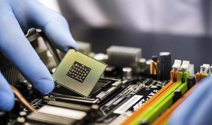
Georgia Tech Receives $65 Million Grant from Semiconductor Research Corporation for JUMP 2.0 Centers
Jan 05, 2023 — Atlanta, GA

Georgia Tech was awarded $65.7 million to launch two new JUMP 2.0 research centers. For the photo at bottom: Arijit Raychowdhury (left) and Saibal Mukhopadhyay (center) will lead the two centers. Muhannad Bakir (right) is associate director of a third center headquartered at Penn State.
Intelligent machines and AI characters that can interact seamlessly and intimately with human beings will have wide-ranging effects on society – in healthcare, search and rescue, business and defense, and even recreation. The technology is not very far off, and a massive national effort, led in part by Georgia Tech researchers, is charting the course.
Last year, the Semiconductor Research Corporation (SRC) and the Defense Advanced Research Projects Agency (DARPA) announced a new program to improve the nation’s information and technology infrastructure. With a global chip shortage, supply chain issues, and other challenges in play, a group of Georgia Tech faculty members jumped at the opportunity to participate.
Their landing was perfect. Two new research centers, representing an investment of about $65.7 million, have been awarded to Georgia Tech through the SRC-administrated Joint University Microelectronics Program 2.0, or JUMP 2.0.
JUMP 2.0 will support the work of dozens of inter-disciplinary researchers from multiple universities, tackling the technological issues of an increasingly connected world. The goal is to improve the nation’s performance, efficiency, and capabilities for both commercial and military applications.
“Georgia Tech won two of the seven centers, which is not only fantastic, but also speaks highly about the breadth and depth of our research enterprise,” said Professor Arijit Raychowdhury, the Steve W. Chaddick Chair of the School of Electrical and Computer Engineering at Georgia Tech, who will direct one of the new centers.
The JUMP 2.0 announcement represents the latest round of significant support advancing AI-related research at Georgia Tech. Last July, Tech received two National Science Foundation Artificial Intelligence Research awards totaling $40 million. In September, the U.S. Economic Development Administration awarded Georgia Tech $65 million to support a statewide initiative combining AI and manufacturing innovations with workforce and outreach programs.
A New Collaborative Chapter
Launching in 2023, JUMP 2.0 is the next chapter of an SRC-led alliance that formed in 2018 – the original JUMP, with its broad focus on nano-electronic computing.
JUMP 2.0 is a collaboration between SRC industrial participants (IBM, Intel, Raytheon, TSMC and Samsung, to name a few) and the Department of Defense. The program asked researchers from U.S. universities to solicit proposals for collaborative, multidisciplinary, multi-institute research in seven theme areas: cognition; communications and connectivity; intelligent sensing to action; systems and architectures for distributed computing; intelligent memory and storage; advanced monolithic and heterogenous integration; and high-performance energy efficient devices.
The two new research centers Georgia Tech, both headquartered within the School of Electrical and Computer Engineering (ECE) are:
• CoCoSys: Center for the Co-Design of Cognitive Systems (theme area: cognition), under the direction of Raychowdhury;
• CogniSense: Center on Cognitive Multispectral Sensors (theme area: intelligent sensing to action), under the direction of Saibal Mukhopadhyay, Joseph M. Pettit Professor in ECE.
Semiconductors, or microchips, are basically tiny silicon slices packed with millions of transistors that control electron activity. These chips enable all our electronic devices to work. So, a shortage of semiconductors – or a shortcoming in terms of quality and efficiency – spells trouble for sectors and industries that depend on these little bits of hardware, for example: computing, healthcare, telecommunication, security, transportation, or manufacturing.
Building a Digital Human
The goals for the JUMP 2.0 centers are lofty and wide-ranging, addressing current and future needs.
“In some sense, the question we’re addressing is, ‘how do you build a perfect digital human,’” Raychowdhury said of the Team CoCoSys mission. “We want to learn how to build systems which are aware – capable of interacting as human agents with us. For example, we want AI that can listen to a conversation between two human beings and learn from that and seamlessly merge into society.”
Current AI, Raychowdhury said, may be able to perform relatively narrow tasks better than a human, but one area that it is much less effective is human-intelligent machine collaboration. This concept has been increasingly researched in recent years as automated virtual assistants and the metaverse have entered the mainstream. As cognitive systems research moves toward creation of a digital human, it will have far-reaching impact in industry and healthcare testing, disaster relief, fully autonomous and collaborative systems, immersive training and gaming experiences, and more.
“Continuous learning through interactions with humans is missing,” Raychowdhury said. “The next generation of AI needs to comprehend nuances of human interaction, explain, and interpret visual cues and language, and be able to do that in real-time with high energy-efficiency. That’s what we want to address. That’s the meta goal of this center.”
Three other Georgia Tech faculty researchers, all from ECE, are part of Team CoCoSys: Larry Heck, Azad Naeemi, and Tushar Krishna.
“This is a diverse team in all possible ways with expertise across the board,” Raychowdhury said.
Sensors with a Brain
The ability to sense is fundamental and probably the most critical component for building an intelligent machine. “It is fundamental to nature,” said Mukhopadhyay. “We have eyes, ears, a nose, and skin to sense the environment around us.”
The CogniSense Center research team wants to develop sensors that can effectively “perceive” everything around them and, like humans, efficiently attend to the information that really matters.
Today’s electronics sensors samples everything they “see” and generate abundance of digital data; sometime way too much for a machine store, process, and make sense. The CogniSense center’s goal is to change this paradigm by learning from biology.
“In human, sensors and the brain work together to control attention and extract only important information from everything happening around us,” said Mukhopadhyay. “Can we make electronic sensors that behave like that – cognizant and energy efficient?”
The team he’s assembled is made up of 20 researchers from 12 different institutions, including two other ECE faculty members: Justin Romberg (associate chair for research in ECE) and Muhannad Bakir (interim director of the Georgia Tech 3D Systems Packing Research Center).
“We have a diverse team with expertise in radars, optics, integrated circuits, packaging, signal processing, and artificial intelligence to build these new sensors with a brain,” said Mukhopadhyay.
Beyond Campus
Georgia Tech researchers will play critical roles in three other centers based at other universities around the country:
• PRISM: Center for Processing with Intelligent Storage and Memory
• ACE: Evolvable Computing for Next-Generation Distributed Computer Systems.
• CHIMES: Center for Heterogenous Integration of Microelectronic Systems
CHIMES in particular will feature a large, multi-disciplinary Georgia Tech influence including ECE’s Suman Datta, Callie Hao, and Shimeng Yu; George Woodruff School of Mechanical Engineering’s Suresh Sitaraman and Satish Kumar; and the center’s associate director, Bakir (doubling up on his JUMP 2.0 responsibilities as a member of both CogniSense and CHIMES).
“We are delighted in the critical and fundamental role Georgia Tech plays within CHIMES,” said Bakir. “In each of the four research themes that constitute this center, Georgia Tech faculty play a key role. This not only reflects our world class faculty, students, and staff, but also our world-class fabrication, assembly and bonding, and advanced system level prototyping facilities that will be critical in enabling next generation 3D heterogeneous and 3D monolithic circuits and systems.”
Establishing all of these new semiconductor research centers is the result of impeccable timing, according to Raychowdhury, who pointed out that ECE broke into the top two in national rankings by U.S. News and World Report rankings for the first time in 2022, not long after President Biden signed the CHIPS and Science Act, which provides about $280 billion in new funding to boost U.S. research and manufacturing of semiconductors.
“These research centers are part of a confluence of things that are happening simultaneously across the U.S.,” he said. “And they have implications for Georgia Tech, national security, and the independence of our national supply chain as a whole.”
Writer: Jerry Grillo
At the Edge of Graphene-Based Electronics
Jan 03, 2023 — Atlanta, GA

Claire Berger, physics professor at Georgia Tech, holds the team's graphene device grown on a silicon carbide substrate chip. Credit: Jess Hunt-Ralston, Georgia Tech
A pressing quest in the field of nanoelectronics is the search for a material that could replace silicon. Graphene has seemed promising for decades. But its potential faltered along the way, due to damaging processing methods and the lack of a new electronics paradigm to embrace it. With silicon nearly maxed out in its ability to accommodate faster computing, the next big nanoelectronics platform is needed now more than ever.
Walter de Heer, Regents’ Professor in the School of Physics at the Georgia Institute of Technology, has taken a critical step forward in making the case for a successor to silicon. De Heer and his collaborators developed a new nanoelectronics platform based on graphene — a single sheet of carbon atoms. The technology is compatible with conventional microelectronics manufacturing, a necessity for any viable alternative to silicon. In the course of their research, published in Nature Communications, the team may have also discovered a new quasiparticle. Their discovery could lead to manufacturing smaller, faster, more efficient, and more sustainable computer chips, and has potential implications for quantum and high-performance computing.
“Graphene’s power lies in its flat, two-dimensional structure that is held together by the strongest chemical bonds known,” de Heer said. “It was clear from the beginning that graphene can be miniaturized to a far greater extent than silicon — enabling much smaller devices, while operating at higher speeds and producing much less heat. This means that, in principle, more devices can be packed on a single chip of graphene than with silicon.”
In 2001, de Heer proposed an alternative form of electronics based on epitaxial graphene, or epigraphene — a layer of graphene that was found to spontaneously form on top of silicon carbide crystal, a semiconductor used in high power electronics. At the time, researchers found that electric currents flow without resistance along epigraphene’s edges, and that graphene devices could be seamlessly interconnected without metal wires. This combination allows for a form of electronics that relies on the unique light-like properties of graphene electrons.
“Quantum interference has been observed in carbon nanotubes at low temperatures, and we expect to see similar effects in epigraphene ribbons and networks,” de Heer said. “This important feature of graphene is not possible with silicon.”
Building the Platform
To create the new nanoelectronics platform, the researchers created a modified form of epigraphene on a silicon carbide crystal substrate. In collaboration with researchers at the Tianjin International Center for Nanoparticles and Nanosystems at the University of Tianjin, China, they produced unique silicon carbide chips from electronics-grade silicon carbide crystals. The graphene itself was grown at de Heer’s laboratory at Georgia Tech using patented furnaces.
The researchers used electron beam lithography, a method commonly used in microelectronics, to carve the graphene nanostructures and weld their edges to the silicon carbide chips. This process mechanically stabilizes and seals the graphene’s edges, which would otherwise react with oxygen and other gases that might interfere with the motion of the charges along the edge.
Finally, to measure the electronic properties of their graphene platform, the team used a cryogenic apparatus that allows them to record its properties from a near-zero temperature to room temperature.
Observing the Edge State
The electric charges the team observed in the graphene edge state were similar to photons in an optical fiber that can travel over large distances without scattering. They found that the charges traveled for tens of thousands of nanometers along the edge before scattering. Graphene electrons in previous technologies could only travel about 10 nanometers before bumping into small imperfections and scattering in different directions.
“What's special about the electric charges in the edges is that they stay on the edge and keep on going at the same speed, even if the edges are not perfectly straight," said Claire Berger, physics professor at Georgia Tech and director of research at the French National Center for Scientific Research in Grenoble, France.
In metals, electric currents are carried by negatively charged electrons. But contrary to the researchers’ expectations, their measurements suggested that the edge currents were not carried by electrons or by holes (a term for positive quasiparticles indicating the absence of an electron). Rather, the currents were carried by a highly unusual quasiparticle that has no charge and no energy, and yet moves without resistance. The components of the hybrid quasiparticle were observed to travel on opposite sides of the graphene’s edges, despite being a single object.
The unique properties indicate that the quasiparticle might be one that physicists have been hoping to exploit for decades — the elusive Majorana fermion predicted by Italian theoretical physicist Ettore Majorana in 1937.
“Developing electronics using this new quasiparticle in seamlessly interconnected graphene networks is game changing,” de Heer said.
It will likely be another five to 10 years before we have the first graphene-based electronics, according to de Heer. But thanks to the team’s new epitaxial graphene platform, technology is closer than ever to crowning graphene as a successor to silicon.
Citation: Prudkovskiy, V.S., Hu, Y., Zhang, K. et al. An epitaxial graphene platform for zero-energy edge state nanoelectronics. Nat Commun 13, 7814 (2022).
DOI: 10.1038/s41467-022-34369-4
Writer: Catherine Barzler
Photography: Jess Hunt-Ralston
The Georgia Institute of Technology, or Georgia Tech, is one of the top public research universities in the U.S., developing leaders who advance technology and improve the human condition. The Institute offers business, computing, design, engineering, liberal arts, and sciences degrees. Its more than 46,000 students, representing 50 states and more than 150 countries, study at the main campus in Atlanta, at campuses in France and China, and through distance and online learning. As a leading technological university, Georgia Tech is an engine of economic development for Georgia, the Southeast, and the nation, conducting more than $1 billion in research annually for government, industry, and society.
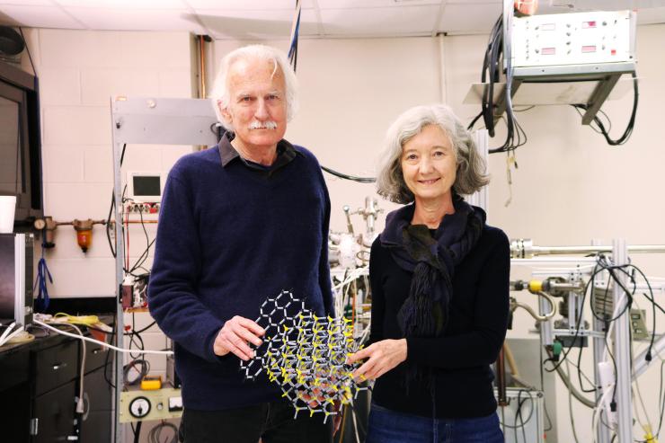
Walter de Heer and Claire Berger, physics professors, holding an atomic model of graphene (black atoms) on crystalline silicon carbide (yellow atoms) in the Epitaxial Graphene Lab at Georgia Tech. Credit: Jess Hunt-Ralston, Georgia Tech

De Heer's patented induction furnace used to produce graphene on silicon carbide. Credit: Jess Hunt-Ralston, Georgia Tech
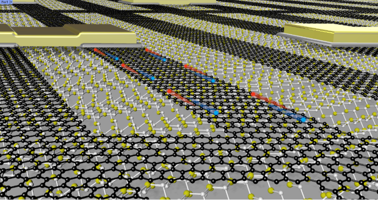
Art which depicts the graphene network (black atoms) on top of silicon carbide (yellow and white atoms). The gold pads represent electrostatic gates, and the blue and red balls represent electrons and holes, respectively. Credit: Noel Dudeck, Georgia Tech
Catherine Barzler, Senior Research Writer/Editor
Georgia Tech Remains in Top 20 in Higher Education Research Spending
Dec 20, 2022 — Atlanta, GA

Annual research spending enables medical breakthroughs, space exploration, and scientific innovation across multiple disciplines
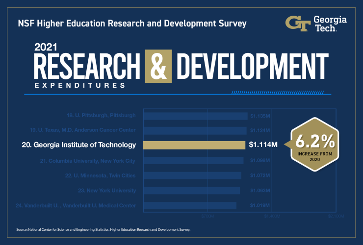
For the second consecutive year, the Georgia Institute of Technology has garnered a spot among the 20 universities in the U.S. with the highest amount of research and development (R&D) spending. Georgia Tech ranked No. 20, based on the annual Higher Education Research and Development Survey conducted by the National Science Foundation (NSF). The ranking is especially significant because Georgia Tech is the only institution in the Top 20 without a medical school.
Indeed, the research funding has led to remarkable breakthroughs in biomedicine, such as 3D-printed medical devices, including tracheal and bronchial splints for children with rare, life-threatening genetic irregularities. It also has put Georgia Tech at the forefront of sustainability as researchers reimagine toilet systems that operate without inlet water or output sewer lines, improving issues with sanitation and pollution.
“We strive for knowledge, understanding, and impact in all that we do at Georgia Tech,” said Chaouki T. Abdallah, executive vice president for Research at Georgia Tech. “These expenditures also help us address our most pressing challenges here at home in Georgia, around the world, and even beyond Earth.”
The research has also taken Georgia Tech to space with a team of faculty and students guiding NASA’s Lunar Flashlight satellite probe in the quest to find frozen water on Earth’s moon. Here at home, Georgia Tech is leading a coalition of partners across the state in an effort to bring together artificial intelligence and innovation to strengthen Georgia’s manufacturing sector, create new opportunities for the state’s workforce, and augment its economic resiliency.
Georgia Tech’s R&D spending of $1.114 billion in fiscal year 2021 reflects a 6.2% increase from the 2020 figure for its entire research enterprise, which includes the Georgia Tech Research Institute (GTRI). All R&D spending in higher education increased 4% to $89.872 billion in fiscal year 2021. The nation’s top 30 schools accounted for 42% of that overall R&D spending amount, unchanged from 2020.
"We are proud to see Georgia Tech in such a distinguished group of public and private universities,” said Abdallah. “The driving mission behind all of our research is to develop and lead in creative work and innovations that improve the human condition.”
The NSF collected its data from 916 universities in the Higher Education Research and Development Survey, sponsored by the NSF’s National Center for Science and Engineering Statistics unit.
The Institute’s showing on the list of research-intensive or R1 universities places it among a group of schools that include Johns Hopkins University, which had the top spot in R&D spending with $3.181 billion, Duke University (No. 11 with $1.237 billion), and Yale University (No. 15 with $1.165 billion).
In addition to the innovations that those federal and state research dollars and foundation grants help support, the R&D funding has very real and immediate impact on Georgia’s economy. According to the University System of Georgia, all schools within the system contributed $19.3 billion to the state’s economy in fiscal year 2021. Georgia Tech’s portion of that total — roughly $4.2 billion — was the highest of any USG institution and reflects a 4.6% jump from fiscal year 2020. Learn more about Georgia Tech’s research contributions in this report.
Péralte C. Paul
peralte.paul@comm.gatech.edu
404.316.1210
GEDC Distinguished Lecture Series | When Optics met Digital Signal Processing: a Love Story
Featuring Kim Robers, Vice President, WaveLogic Science, Ciena and Ian Roberts, DSP Engineer, Ciena
Nano@Tech Spring 2023 Series | Self-Assembly of Bioresource Materials for Functional Nanoparticles
Featuring Zhaohui (Julene) Tong | School of Chemical and Biomolecular Engineering at Georgia Tech
Abstract: Bioresource materials such as cellulose, chitin, and lignin, are usually low-cost, biocompatible, and abundant in nature. The synthesis of functional materials from these bioresource materials can address long-term environmental challenges such as resource and energy depletion, plastic pollution, and climate change.
Faces of Research: Meet Mark Prausnitz
Jan 05, 2023 — Atlanta, GA

Georgia Tech’s School of Chemical and Biomolecular Engineering is a leader in the field of chemical and biomolecular engineering. Its mission is to create a better future by transforming people, ideas, processes and products through research and innovations that will transform the lives of its students and generate breakthroughs in technology and knowledge.
This installment of the Faces of Research Q&A series is with Mark Prausnitz, Regents' Professor, J. Erskine Love Jr. Chair in Chemical and Biomolecular Engineering, and Director of the Center for Drug Design, Development and Delivery.
What is your field of expertise and why did you choose it?
In my lab, we work in the field of pharmaceuticals. We design drug delivery systems to make drugs work better and to make them more accessible to people by simplifying their administration at home, in developing countries, and in emergency situations. The main technology we study is microneedles. We make microneedle patches, which are painlessly applied to the skin to administer drugs and vaccines without the need for hypodermic injections. We also make particles with microneedles sticking out called STAR particles that can be rubbed onto the skin to increase absorption of dermatological drugs and cosmetics. We also work on microneedles for targeted injection into the eye to treat diseases like macular degeneration. I became interested in this work because I can use my training in engineering to solve problems that improve the health of people in the United States and around the world. I also enjoy working in the area of pharmaceuticals because of its interdisciplinary nature, drawing not only from science and engineering, but also from medicine, public health, public policy, and other fields.
What makes Georgia Tech research institutes unique?
I was initially attracted to Georgia Tech, and remain excited about being here, because of the emphasis on interdisciplinary research and collaboration, especially at the interface of engineering and medicine. These days, many research institutions talk about interdisciplinary research, but Georgia Tech has been a leader in this area for decades and had a world-class environment to collaborate across disciplines to do innovative and impactful research. For me, collaboration with Emory University and the CDC are additional critical features of the Georgia Tech research environment.
What impact is your research having on the world?
We had our first product approved by Food and Drug Administration in 2021. It is a microneedle that administers a drug into a part of the eye called the suprachoroidal space to treat inflammation of the eye with reduced side effects as compared to conventional treatments. We also have studied microneedle patches in a number of clinical trials, including administration of influenza vaccine and measles and rubella vaccines. I have co-founded eight companies to commercialize the drug delivery systems we have developed at Georgia Tech. Publishing high-quality research and training students are very important to me; moving our technology out of the Institute and into clinical use that helps people is also important.
What is something you wished you knew as a budding researcher that everyone considering research as a career should know?
My graduate mentor advised me that a good researcher knows how to design a study, carry out research, interpret results, and get the answer to a scientific question. But a great researcher knows which scientific question to ask. I think picking the right research questions is the key to doing impactful research.
What is the most challenging aspect of your research?
The most challenging and most important component of my research is the research team. We encounter many technical challenges, but if we have the right people working in the right environment, we can overcome those challenges. I think it is important to recruit smart, enthusiastic, and hard-working graduate students and postdocs, and then create a physical, intellectual, and cultural environment that allow them and their research to thrive.
Favorite show/program to binge watch?
My introduction to binge watching was Breaking Bad, which is ultimately a show about drug delivery (although not the kind that we do, of course!). I like history, so I watch The Crown. I also like mysteries, and am eagerly awaiting the next season of Only Murders in the Building. Currently, I am watching Ted Lasso to wind down after a busy day.
Peralte C. Paul
peralte.paul@comm.gatech.edu
404.316.1210