ASPE 2023 Spring Topical Meeting on Precision Micro-Nano Technology
April 20-21, 2023
Call for Papers
The 2023 Spring Topical Meeting will connect precision micro-nano engineering experts from academia, industry and national labs, with each group finding value in attending this topical meeting.
Nano@Tech Spring 2023 Series | An Engineer’s Perspective on Antiferromagnetic Spintronics
Featuring Assistant Professor Shaloo Rakheja, University of Illinois at Urbana-Champaign
Abstract: Antiferromagnets (AFM) materials have ordered spin moments that alternate between individual atomic sites, which gives them a vanishing macroscopic magnetic signature and picosecond intrinsic timescale.
Faces of Research: Meet Chaouki T. Abdallah
Feb 16, 2023 — Atlanta, GA

The $1.3 billion research enterprise at Georgia Tech is the embodiment of a commitment the advancement of technology and betterment of the human condition. Georgia Tech's research enterprise through offerings such as the Enterprise Innovation Institute, the Georgia Tech Research Institute, Commercialization, and Interdisciplinary Research Institutes, to solve the most pressing challenges in a host of sectors, including computing, engineering, design, the sciences, liberal arts, and business.
This installment of the Faces of Research Q&A series is with Chaouki T. Abdallah, Executive Vice President for Research at Georgia Tech.
What is your field of expertise and why did you choose it?
My field of expertise is Systems Theory, and my degrees are all in Electrical Engineering. I chose it because it was heavily mathematical but can also be applied across multiple fields (aerospace, chemical, mechanical, electrical, biology, etc.).
What makes Georgia Tech research institutes unique?
Our IRIs (Interdisciplinary Research Institutes) connect research across colleges but what makes them even more impactful is their intra-connectivity. Problems that are even too big for one IRI, are being solved by researchers across multiple ones.
What impact is your research having on the world?
My own research impact has been mostly through my students. However, I did use my research in systems and network science to study and improve the complexity of college curricula, leading to 150% improvement in the four-year graduation rate and tens of millions of dollars in savings for students.
What is the most profound advice you ever received?
Pick the hill you’re willing to die on.
What is something you wished you knew as a budding researcher that everyone considering research as a career should know?
The joy of knowing something is eclipsed by the joy of explaining it to others.
What song or album best describes you?
"With a Little Help From My Friends" by The Beatles.
News Contact
Péralte C. Paul
404.316.1210
peralte.paul@comm.gatech.edu
Georgia Electronic Design Center Distinguished Lecture Series | The Role of Electronically Reconfigurable, Reflectarrays, Transmitarrays, and Metasurfaces in Future Phased-Array Antenna Applications
Featuring Nader Behdad, McFarland-Bascom Professor, Department of ECE at the University of Wisconsin-Madison
Host: Nima Ghalichechian
Abstract: Phased-array antennas are widely used in various communications, radar, and electronic warfare systems. Compared to mechanically beam-steerable antennas, they provide significantly faster beam steering and more functionalities albeit at the expense of added cost and complexity of design. Phased-array antennas can be categorized into active and passive electronically steered arrays (AESAs and PESAs).
Science & Engineering Day at Georgia Tech
Once again, the Atlanta Science Festival is looking forward to painting the city with science in March 2023. Stay tuned for the schedule release for the 2023 Festival in February!
The Festival is engineered by Science ATL and community partners, with major support from founders Emory University, Georgia Tech, and the Metro Atlanta Chamber, and from sponsors UPS, International Paper, Georgia Power, Cox Enterprises, Lockheed Martin, Lenz Marketing, and Mercer University.
Mark Prausnitz Elected to National Academy of Engineering
Feb 09, 2023 — Atlanta, GA

Professor and entrepreneur Mark Prausnitz has been elected to the National Academy of Engineering (NAE), joining a membership that includes the nation’s most distinguished engineers. He is Georgia Tech’s 46th NAE member.
Prausnitz is the J. Erskine Love Jr. Chair of the School of Chemical and Biomolecular Engineering (ChBE) and director of Georgia Tech’s Center for Drug Design, Development and Delivery. He’s also the only Georgia Tech faculty member recognized as both a Regents’ Professor and Regents’ Entrepreneur, the highest academic titles awarded by the University System of Georgia Board of Regents. He joins 105 new NAE members in the 2023 class along with 18 new international members.
News Contact
Jason Maderer
College of Engineering
Researchers Pioneer Process to Stack Micro-LEDs
Feb 09, 2023 — Metz, France
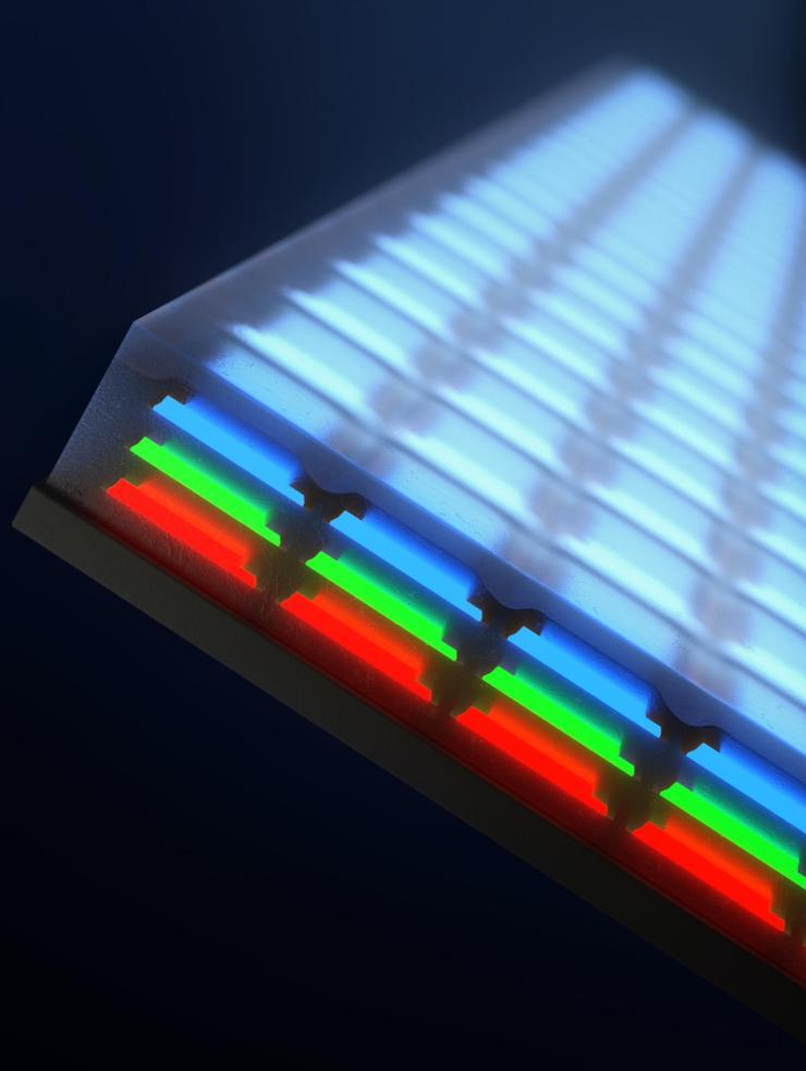
Illustration of stacked LEDs (Credit: Younghee Lee)
Put on a virtual reality headset and, chances are, it will look like you are viewing the world through a screen door. Current flat panel displays use pixels that are visible to the naked eye, along with small bits of unlit dark space between each pixel that can appear as a black, mesh-like grid.
Now, researchers from the Georgia Institute of Technology, in collaboration with researchers from the Massachusetts Institute of Technology (MIT), have developed a new process based on 2D materials to create LED displays with smaller and thinner pixels. Enabled by two-dimensional, materials-based layer transfer technology, the innovation promises a future of clearer and more realistic LED displays.
The team published a paper in the journal Nature in February titled, “Vertical full-colour micro-LEDs via 2D materials-based layer transfer.” Co-authors also include researchers from Sejong University in Korea, and from additional institutions in the U.S. and South Korea.
Georgia Tech-Europe Professor Abdallah Ougazzaden and research scientist Suresh Sundaram (who both also hold appointments in Georgia Tech’s School of Electrical and Computer Engineering) collaborated with researchers from MIT to turn the conventional LED manufacturing process on its head — literally. Instead of using prevailing processes based on laying red, green, and blue (RGB) LEDs side by side, which limits pixel density, the team vertically stacked freestanding, ultrathin RGB LED membranes, achieving an array density of 5,100 pixels per inch — the smallest pixel size reported to date (4 microns) and the smallest-ever stack height — all while delivering a full commercial range of colors. This ultra-small vertical stack was achieved via the technology of van der Waals epitaxy on 2D boron nitride developed at the Georgia Tech-Europe lab and the technology of remote epitaxy on graphene developed at MIT.
The study showed that the world’s thinnest and smallest pixeled displays can be enabled by an active layer separation technology using 2D materials such as graphene and boron to enable high array density micro-LEDs resulting in full-color realization of micro-LED displays.
One unique facet of the two-dimensional, material-based layer transfer (2DLT) technique is that it allows the reuse of epitaxial wafers. Reusing this costly substrate could significantly lower the cost for manufacturing smaller, thinner, and more realistic displays.
“We have now demonstrated that this advanced 2D, materials-based growth and transfer technology can surpass conventional growth and transfer technology in specific domains, such as in virtual and augmented reality displays,” said Ougazzaden, the lead researcher for the Georgia Tech team.
These advanced techniques were developed in metalorganic chemical vapor deposition (MOCVD) reactors, the key tool for LED production at the wafer scale. The 2DLT technique can be replicated on an industrial scale with high throughput yield. The technology has the potential to bring the field of virtual and augmented reality to the next level, enabling the next generation of immersive, realistic micro-LED displays.
“This emerging technology has a tremendous potential for flexible electronics and the heterogenous integration in opto-electronics, which we believe will develop new functionalities and attract industry to develop commercial products from smartphone screens to medical devices,” Ougazzaden said.
Citation: Shin, J., Kim, H., Sundaram, S. et al. Vertical full-colour micro-LEDs via 2D materials-based layer transfer. Nature 614, 81–87 (2023).
News Contact
Andrea Gappell, Communications Program Manager for GT-Europe
Seeking Demonstration Groups for GT Science and Engineering Day
Feb 02, 2023 — Atlanta, GA

On Saturday, March 11, 2023, Georgia Tech will open its doors to the community for Science and Engineering Day at Georgia Tech.
This annual event aims to inspire the next generation of engineers and scientists and share the breadth of Georgia Tech’s research activities with the local community. Last year more than 500 attendees, ranging from toddlers to retirees, explored the campus and participated in hands-on STEAM activities, tours, and demonstrations designed to engage and educate participants. While attendees were able to get a glimpse into one of the nation’s most research-intensive universities, the community-wide event also allowed Georgia Tech students, researchers, and staff members the opportunity to share their work with the public.
Seeking Demo Groups
To continue the success of Science and Engineering Day, we need members of the Georgia Tech community — including student groups, labs, staff, and faculty — to participate in this year’s event. Last year, 26 units and student organizations across campus provided activities in biology, space, art, nanotechnology, paper, computer science, wearables, bioengineering, and chemical engineering just to name a few.
Taking part in Science and Engineering Day gives Georgia Tech students and researchers a unique opportunity to share their work with the community and inspire attendees. Demo space is limited, so reserve your spot today. Opportunities include hands-on STEAM activities, exhibits, demonstrations, and opportunities to meet student researchers. If you have questions about how you can participate, reach out to Leslie O’Neil. All demo groups must register by February 20, 2023.
The Atlanta Science Festival is engineered by Science ATL and community partners, with major support from founders Emory University, Georgia Tech, and the Metro Atlanta Chamber, and from sponsors UPS, International Paper, Georgia Power, Cox Enterprises, Lockheed Martin, Lenz Marketing, and Mercer University.
Learn more and register to demonstrate at research.gatech.edu/ATLscifestGTday23
News Contact
Spring 2023 IEN Microfabrication Short Course
IEN Microfabrication Short Course
The Institute for Electronics and Nanotechnology (IEN) at Georgia Tech will offer a short course on microfabrication on March 23 - 24, 2023. This intensive two-day short course combines classroom lectures and laboratory based hands-on fabrication in the IEN cleanroom. The goal of the course is to impart a basic understanding of the science and technology of microfabrication processes as used in academia and industry.